CO.,LTD")
Hersteller von Ajinomoto GXT31R2-Paketsubstraten. Der Hersteller von Ajinomoto GXT31R2-Paketsubstraten ist auf die Herstellung hochmoderner Substrate für die Elektronik spezialisiert Verpackung Lösungen. Mit einem Engagement für Präzisionstechnik und Innovation, Sie entwickeln sorgfältig Substrate, die auf die Anforderungen moderner elektronischer Geräte zugeschnitten sind. Ihre GXT31R2-Serie ist ein Beispiel für ihr Engagement für Qualität, bietet Zuverlässigkeit und Leistung in jeder Komponente. Als vertrauenswürdiger Name in der Branche, Ajinomoto stellt sicher, dass seine Substrate strengen Standards entsprechen, Dies garantiert optimale Funktionalität und Haltbarkeit für ein vielfältiges Anwendungsspektrum. Vertrauen Sie Ajinomoto GXT31R2 für erstklassige Gehäusesubstratlösungen, die die Technologie von morgen vorantreiben.
Was ist das Ajinomoto GXT31R2-Paketsubstrat??
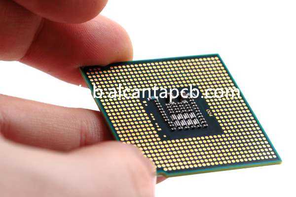
Ajinomoto GXT31R2 Paketsubstrat ist einer der lebenswichtigen Grundbestandteile elektronischer Geräte. Es übernimmt die zentrale Aufgabe, elektronische Komponenten zu verbinden und zu unterstützen, Bereitstellung einer zuverlässigen Grundlage für den normalen Betrieb verschiedener elektronischer Geräte. Dieses Substrat verwendet Ajinomoto GXT31R2-Material, ein erstklassiges Material mit hervorragender Wärmeleitfähigkeit, elektrische Leistung und mechanische Festigkeit.
Erste, Das Ajinomoto GXT31R2-Gehäusesubstrat verbindet die elektronischen Komponenten über leitende Pfade und bildet so einen vollständigen Schaltkreis. Diese Leiterbahnen sind präzise auf der Oberfläche des Substrats angeordnet, um die Stabilität und Zuverlässigkeit der Signalübertragung zu gewährleisten. Diese Verbindungsmethode ist zuverlässiger als herkömmliche Verkabelungsmethoden und ermöglicht die Integration von mehr elektronischen Komponenten auf kleinerem Raum, Dadurch wird die Leistung und Funktionalität des Geräts verbessert.
Zweitens, Das Ajinomoto GXT31R2-Gehäusesubstrat dient als Stützstruktur für elektronische Komponenten und ist unter verschiedenen Umgebungsbedingungen mechanischen Belastungen und Vibrationen ausgesetzt. Das Material Ajinomoto GXT31R2 verfügt über eine hervorragende mechanische Festigkeit und kann elektronische Komponenten wirksam vor der äußeren Umgebung schützen und einen stabilen Betrieb der Ausrüstung unter verschiedenen Arbeitsbedingungen gewährleisten.
Zusätzlich, Das Material Ajinomoto GXT31R2 verfügt außerdem über hervorragende Wärmeleitfähigkeitseigenschaften, Dadurch kann die von elektronischen Bauteilen erzeugte Wärme effektiv zum Kühlkörper oder Gerätegehäuse geleitet werden, um eine stabile Leistung und langfristige Zuverlässigkeit des Geräts zu gewährleisten. Dies ist besonders wichtig für leistungsstarke elektronische Geräte, insbesondere in Arbeitsumgebungen mit hohen Temperaturen. Es kann die Betriebstemperatur von Komponenten effektiv senken und die Lebensdauer der Ausrüstung verlängern.
Zusammenfassend, Das Ajinomoto GXT31R2-Gehäusesubstrat ist eine Grundkomponente mit hervorragender Leistung und Zuverlässigkeit, die in elektronischen Geräten eine unersetzliche Rolle spielt. Durch die Verwendung von Verpackungssubstraten aus hochwertigen Ajinomoto GXT31R2-Materialien, Es kann eine stabile Leistung des Geräts gewährleistet werden, zuverlässiger Betrieb und lange Lebensdauer, so treffen benutzer’ hohe Anforderungen an die Qualität und Leistung elektronischer Produkte.
Ajinomoto GXT31R2-Paket-Substrat-Design-Referenzhandbuch.
Das Ajinomoto GXT31R2-Gehäusesubstrat ist eine Kernkomponente moderner elektronischer Geräte, und sein Design ist entscheidend. Dieses Referenzhandbuch befasst sich mit den Designprinzipien und Best Practices des Ajinomoto GXT31R2-Gehäusesubstrats, um Ingenieuren dabei zu helfen, während des Designprozesses bessere Ergebnisse zu erzielen.
Komponentenlayout: Beim Entwurf des Ajinomoto GXT31R2-Gehäusesubstrats, Eine sinnvolle Komponentenanordnung ist entscheidend. Ein gutes Layout gewährleistet die Signalintegrität, minimiert Signalstörungen, und erleichtert die Wärmeableitung. Ingenieure sollten Faktoren wie die Komponentenfunktionalität berücksichtigen, Zusammenhänge, thermische Anforderungen, und Wartbarkeit.
Signalintegrität: Die Aufrechterhaltung der Signalintegrität ist eines der Hauptziele bei der Entwicklung des Ajinomoto GXT31R2-Gehäusesubstrats. Durch sinnvolle Verkabelungsplanung, Trennung von Masseleitungen und Signalleitungen, und differenzielle Signalverarbeitung, Signalverzerrung, Übersprechen, und Taktjitter können reduziert werden, Dadurch wird die Systemleistung verbessert.
Thermalmanagement: Das Ajinomoto GXT31R2-Gehäusesubstrat weist eine gute Wärmeleitfähigkeit auf, In Hochleistungsanwendungen ist jedoch weiterhin ein effektives Wärmemanagement erforderlich. Designer können Kühlkörper verwenden, Kühlkörper, Wärmeableitungs-Backplanes, usw. um sicherzustellen, dass elektronische Komponenten beim Arbeiten eine stabile Temperatur aufrechterhalten können.
Herstellbarkeit: Beim Entwurf des Ajinomoto GXT31R2-Gehäusesubstrats, Machbarkeit und Effizienz des Herstellungsprozesses müssen berücksichtigt werden. Ingenieure sollten versuchen, den Herstellungsprozess zu vereinfachen, die Herstellungskosten senken, und stellen Sie sicher, dass das Design den Anforderungen des PCB-Herstellungsprozesses entspricht, um die Produktionseffizienz und Produktqualität zu verbessern.
Materialauswahl: Die Leistung des Ajinomoto GXT31R2-Gehäusesubstrats wird direkt von der Materialauswahl beeinflusst. Ingenieure sollten geeignete Substratmaterialien auswählen, Polstermaterialien, Kupferdicke, usw. Basierend auf den Anwendungsanforderungen, um die Produktleistung und -zuverlässigkeit sicherzustellen.
Testen und Verifizieren: Nachdem der Entwurf abgeschlossen ist, Es müssen strenge Tests und Verifizierungen durchgeführt werden, um sicherzustellen, dass die Leistung und Zuverlässigkeit des Ajinomoto GXT31R2-Gehäusesubstrats den Designanforderungen entspricht. Zu den Testinhalten gehören elektrische Tests, Zuverlässigkeitstests, Prüfung der Umweltanpassungsfähigkeit, usw.
Wartung und Updates: Sobald das Ajinomoto GXT31R2-Gehäusesubstrat in Gebrauch genommen wird, Das Designteam muss weiterhin auf Produktwartung und -aktualisierungen achten. Rechtzeitige Reaktion auf Benutzerfeedback, Leistungsoptimierung und Technologieaktualisierungen können die Wettbewerbsfähigkeit der Produkte und die Benutzerzufriedenheit verbessern.
Indem Sie die oben genannten Designprinzipien und Best Practices befolgen, Ingenieure können Ajinomoto GXT31R2-Verpackungssubstrate besser entwerfen und herstellen, starke Unterstützung für die Leistung, Zuverlässigkeit und Wettbewerbsfähigkeit elektronischer Produkte.
Welches Material wird im Ajinomoto GXT31R2-Paketsubstrat verwendet??
Das Ajinomoto GXT31R2-Gehäusesubstrat verwendet Hochleistungsmaterialien, um die strengen Anforderungen der Elektronikindustrie an die Wärmeleitfähigkeit zu erfüllen, elektrische Leistung und mechanische Festigkeit. Diese Art von Verpackungssubstrat wird häufig in hochwertigen elektronischen Geräten verwendet, wie Smartphones, Computer, Steuerungssysteme für Kraftfahrzeuge, usw. Also, Welches Material wird im Ajinomoto GXT31R2-Gehäusesubstrat verwendet??
Zu den Materialien des Verpackungssubstrats Ajinomoto GXT31R2 gehören hauptsächlich Epoxidharz und Glasfaser. Als einer der Hauptbestandteile des Substrats, Epoxidharz hat eine gute Hitzebeständigkeit, mechanische Festigkeit und chemische Stabilität, Dies kann die Stabilität und Zuverlässigkeit des Verpackungssubstrats in komplexen Arbeitsumgebungen gewährleisten. Gleichzeitig, Epoxidharz kann auch gute elektrische Isolationseigenschaften bieten, Interferenzen und Kurzschlüsse zwischen Stromkreisen wirksam verhindert werden.
Glasfaser dient als Verstärkungsmaterial für Epoxidharz, Dadurch können die mechanische Festigkeit und die Zugeigenschaften des Verpackungssubstrats verbessert werden. Glasfaser zeichnet sich durch geringes Gewicht aus, hohe Festigkeit und Verschleißfestigkeit, wodurch die Haltbarkeit und Schlagfestigkeit des Substrats wirksam verbessert werden kann, bei gleichzeitiger Reduzierung des Gesamtgewichts, Dies kommt dem Leichtbau elektronischer Produkte zugute.
Neben Epoxidharz und Glasfaser, Dem Ajinomoto GXT31R2-Gehäusesubstrat können auch einige spezielle Füllstoffe und Zusatzstoffe zugesetzt sein, um seine Leistung weiter zu verbessern. Diese Füll- und Zusatzstoffe können die Wärmeleitfähigkeit verbessern, Korrosionsbeständigkeit und flammhemmende Eigenschaften des Substrats, um den Anforderungen verschiedener Anwendungsszenarien gerecht zu werden.
Im Allgemeinen, Die im Verpackungssubstrat Ajinomoto GXT31R2 verwendeten Materialien zeichnen sich durch hervorragende Leistung und stabile Qualität aus, kann die hohen Leistungs- und Zuverlässigkeitsanforderungen elektronischer Produkte erfüllen, und bieten eine solide Unterstützung für die Entwicklung der Elektronikindustrie.
Welche Größe haben die Ajinomoto GXT31R2-Paketsubstrate??
Ajinomoto GXT31R2-Gehäusesubstrate sind aufgrund ihres breiten Anwendungsspektrums in verschiedenen Größen erhältlich. Dieses Verpackungssubstrat kann in einer Vielzahl elektronischer Produkte verwendet werden, von winzigen Mobilgeräten bis hin zu großen Industrieanlagen, Daher ist der Größenbereich ziemlich groß.
In kleinen elektronischen Geräten, wie Smartphones, Tabletten, und Wearables, Ajinomoto GXT31R2-Gehäusesubstrate sind oft sehr klein. Ihre Abmessungen dürfen nur wenige Zentimeter mal wenige Zentimeter betragen, um dem kompakten Design und den Miniaturisierungsanforderungen des Geräts gerecht zu werden. Diese kleinen Substrate müssen viele elektronische Komponenten auf begrenztem Raum unterbringen und stabile Verbindungen und eine effiziente Anordnung zwischen ihnen gewährleisten.
Im Vergleich, in großen elektronischen Geräten und Systemen, Das Ajinomoto GXT31R2-Gehäusesubstrat kann größer sein. Zum Beispiel, in industriellen Automatisierungsgeräten, Kommunikationsbasisstationen, und medizinische Bildgebungsgeräte, Verpackungssubstrate müssen möglicherweise größer sein, um mehr elektronische Komponenten und Anschlüsse aufzunehmen. Diese großen Substrate weisen oft komplexere Designs und Layouts auf, um den hohen Leistungs- und Zuverlässigkeitsanforderungen des Geräts gerecht zu werden.
Im Allgemeinen, Die Größe des Ajinomoto GXT31R2-Gehäusesubstrats hängt von den Anforderungen des spezifischen elektronischen Geräts oder Systems ab, auf das es angewendet wird. Ob klein oder groß, Dieses Verpackungssubstrat kann effiziente elektrische Verbindungen und stabile Leistung bieten, Bereitstellung von Support und Lösungen für verschiedene Anwendungsszenarien.
Der Herstellungsprozess des Ajinomoto GXT31R2-Paketsubstrats.
Der Herstellungsprozess des Ajinomoto GXT31R2-Gehäusesubstrats ist ein komplexer und präziser Prozess, der mehrere Schlüsselschritte umfasst, Jeder Schritt ist entscheidend und wirkt sich direkt auf die Qualität und Leistung des Endprodukts aus.
Die erste Phase ist die Vorbereitung des Untergrunds. In diesem Stadium, Das ursprüngliche Untergrundmaterial wird vorbereitet und gereinigt, um sicherzustellen, dass die Oberfläche glatt ist, staubfrei und kontaminationsfrei. Dies ist die Grundlage für den reibungslosen Ablauf nachfolgender Prozesse. Eventuelle Verunreinigungen oder schlechte Bedingungen können während des Herstellungsprozesses zu Problemen führen.
Als nächstes erfolgt die Ebenenausrichtung. In diesem Schritt, Die verschiedenen Materialschichten werden präzise ausgerichtet, um Positionsgenauigkeit und Verbindungssicherheit in den nachfolgenden Verarbeitungsschritten zu gewährleisten. Die Präzisionsausrichtungstechnologie ist einer der Schlüssel zur Herstellung hochwertiger Substrate.
Anschließend erfolgt das Ätzen oder Drucken der Leiterbahnen. In diesem Schritt, Auf der Oberfläche des Substrats werden durch chemische Ätz- oder Drucktechniken leitende Pfade gebildet, die zur Verbindung von Schaltkreisen zwischen elektronischen Bauteilen dienen. Diese Leiterbahnen müssen ein gewisses Maß an Präzision und Qualität aufweisen, um die Zuverlässigkeit der Übertragung elektronischer Signale und Verbindungen zu gewährleisten.
Anschließend erfolgt das Bohren der Bauteillöcher. In diesem Schritt, Für die Montage der elektronischen Komponenten werden Löcher in das Substrat gebohrt, und leitende Pfade werden durch diese Löcher verbunden. Die Größe und Position der Löcher muss genau gesteuert werden, um unterschiedliche Komponentengrößen und -anordnungen zu berücksichtigen.
Als nächstes kommt die Pad-Abdeckung. In diesem Schritt, Mit Pads werden Leiterbahnen und Löcher zum Löten elektronischer Komponenten abgedeckt. Die Qualität der Pads und die Gleichmäßigkeit der Abdeckung sind entscheidend für die Lötzuverlässigkeit und die Verbindungsqualität.
Dann folgt die Montage der Komponenten. In diesem Schritt, Elektronische Komponenten werden präzise auf dem Substrat montiert und mit Leiterbahnen und Pads verbunden. Der Montageprozess erfordert ein hohes Maß an Präzision und Prozesskontrolle, um die korrekte Positionierung der Komponenten und die Zuverlässigkeit der Verbindungen sicherzustellen.
Schließlich kommt die Testphase. In diesem Schritt, Das hergestellte Substrat wird verschiedenen Tests unterzogen, einschließlich elektrischer Prüfungen, Zuverlässigkeitstests, und Funktionstests. Durch diese Tests, Sie können sicherstellen, dass das Substrat den Designanforderungen entspricht und eine gute Leistung und Zuverlässigkeit aufweist.
Zusammenfassend, Die Herstellung des Ajinomoto GXT31R2-Gehäusesubstrats ist ein komplexer und präziser Prozess, der eine präzise Prozesskontrolle und hochwertige Materialien erfordert, um die Zuverlässigkeit und Leistung des Endprodukts sicherzustellen. Nur durch einen strengen Herstellungsprozess können Ajinomoto GXT31R2-Verpackungssubstrate hergestellt werden, die hohe Standards erfüllen, um den Anforderungen verschiedener elektronischer Geräte gerecht zu werden.
Der Anwendungsbereich des Ajinomoto GXT31R2-Paketsubstrats.
Ajinomoto GXT31R2-Verpackungssubstrate spielen heute in verschiedenen Branchen eine Schlüsselrolle, mit einem breiten Anwendungsspektrum in der Unterhaltungselektronik, Automobil, Luft- und Raumfahrt, Medizinprodukte, Kommunikation und industrielle Automatisierung. Diese Anwendungsbereiche und die Rolle des Ajinomoto GXT31R2-Gehäusesubstrats werden im Folgenden ausführlich besprochen.
Im Bereich Unterhaltungselektronik, Ajinomoto GXT31R2-Verpackungssubstrate werden häufig bei der Herstellung verschiedener elektronischer Produkte wie Smartphones verwendet, Tabletten, und Smart-Home-Ausrüstung. Diese Produkte stellen hohe Anforderungen an eine hohe Dichte und hohe Leistung der Leiterplatten, und das Verpackungssubstrat Ajinomoto GXT31R2 können diese Anforderungen erfüllen und den Verbrauchern ein stabiles und zuverlässiges Produkterlebnis bieten.
In der Automobilindustrie, Ajinomoto GXT31R2-Verpackungssubstrate werden zur Herstellung elektronischer Steuerungssysteme für Kraftfahrzeuge verwendet, Unterhaltungssysteme im Fahrzeug, Ausrüstung für das Internet der Fahrzeuge, usw. Mit der kontinuierlichen Verbesserung der Automobilelektronik, Die Anforderungen an die Stabilität und Zuverlässigkeit elektronischer Geräte werden immer höher, und das Verpackungssubstrat Ajinomoto GXT31R2 können in dieser Hinsicht eine wichtige Rolle spielen.
Im Luft- und Raumfahrtbereich, Ajinomoto GXT31R2-Verpackungssubstrate werden zur Herstellung von Avionikgeräten verwendet, Navigationssysteme, Kommunikationsausrüstung, usw. In der Luft- und Raumfahrt werden extrem hohe Anforderungen an den Leichtbau gestellt, hohe Leistung, und hohe Zuverlässigkeit der Ausrüstung, und das Verpackungssubstrat Ajinomoto GXT31R2 können diese Anforderungen erfüllen und wichtige Unterstützung für die Luft- und Raumfahrtindustrie bieten.
Im Bereich medizinischer Geräte, Ajinomoto GXT31R2-Verpackungssubstrate werden zur Herstellung medizinischer Bildgebungsgeräte verwendet, Überwachungsausrüstung, Diagnosegeräte, usw. Medizinische Geräte stellen extrem hohe Anforderungen an die Sicherheit und Stabilität elektronischer Produkte, Das Verpackungssubstrat Ajinomoto GXT31R2 kann eine stabile und zuverlässige Schaltungsunterstützung bieten, um den normalen Betrieb medizinischer Geräte sicherzustellen.
Im Bereich Kommunikation, Ajinomoto GXT31R2-Verpackungssubstrate werden zur Herstellung von Kommunikationsbasisstationsgeräten verwendet, Kommunikationsausrüstung aus optischen Fasern, Satellitenkommunikationsausrüstung, usw. Kommunikationsgeräte stellen extrem hohe Anforderungen an die hohe Leistung und Zuverlässigkeit elektronischer Produkte, und das Verpackungssubstrat Ajinomoto GXT31R2 können diese Anforderungen erfüllen und wichtige Unterstützung für die Kommunikationsbranche bieten.
Im Bereich der industriellen Automatisierung, Ajinomoto GXT31R2-Verpackungssubstrate werden zur Herstellung industrieller Steuerungssysteme verwendet, Robotersysteme, Sensorausrüstung, usw. Industrielle Automatisierungsgeräte stellen hohe Anforderungen an die Haltbarkeit und Stabilität elektronischer Produkte, Das Verpackungssubstrat Ajinomoto GXT31R2 kann eine zuverlässige Schaltungsunterstützung bieten, um den reibungslosen Ablauf der industriellen Produktion sicherzustellen.
Um zusammenzufassen, Das Verpackungssubstrat GXT31R2 von Ajinomoto spielt in verschiedenen Branchen eine Schlüsselrolle, wichtige Stütze für die Stabilität, Zuverlässigkeit und Leistung elektronischer Geräte, und Förderung des technologischen Fortschritts und der Entwicklung in verschiedenen Branchen.
Was sind die Vorteile des Ajinomoto GXT31R2 Paketsubstrats??
Ajinomoto GXT31R2-Gehäusesubstrate zeichnen sich in der Welt der Elektronikfertigung durch ihre überlegene Leistung und zahlreiche Vorteile aus. Im Vergleich zu herkömmlichen Verkabelungsmethoden, es weist in vielerlei Hinsicht einzigartige Vorteile auf.
Erste, Das Ajinomoto GXT31R2-Gehäusesubstrat hat eine kompakte Größe. Sein Design ermöglicht eine kompaktere Anordnung elektronischer Geräte, Dadurch wird Platz gespart und die Ausrüstung wird leichter und tragbarer. Dies ist besonders wichtig für heutige Unterhaltungselektronikprodukte, die auf eine dünne Bauweise abzielen, Leichtigkeit, und Portabilität.
Zweitens, Das Verpackungssubstrat weist eine äußerst hohe Zuverlässigkeit auf. Hergestellt aus hochwertigem Ajinomoto GXT31R2-Material, Es verfügt über eine hervorragende Haltbarkeit und Stabilität, und kann über einen langen Zeitraum stabil betrieben werden, Reduzierung der Geräteausfallrate, und die Produktzuverlässigkeit und -lebensdauer verbessern.
Dritte, Das Ajinomoto GXT31R2-Gehäusesubstrat lässt sich leicht in Massenproduktion herstellen. Der Herstellungsprozess ist relativ einfach und ermöglicht eine effiziente Großserienproduktion, die Herstellungskosten senken, Verbesserung der Produktionseffizienz, und die Marktnachfrage zu befriedigen.
Zusätzlich, Das Verpackungssubstrat reduziert Montagefehler. Durch präzise Design- und Herstellungsprozesse, Durch Montagefehler verursachte Produktmängel können wirksam reduziert werden, Produktionseffizienz verbessert, und Produktionskosten reduziert.
Zusätzlich, Das Ajinomoto GXT31R2-Gehäusesubstrat verbessert die Signalintegrität. Sein Design kann Störungen und Verluste während der Signalübertragung minimieren, Gewährleisten signal stabilität und genauigkeit, und die Systemleistung verbessern.
Endlich, Das Verpackungssubstrat verfügt über hervorragende Wärmeableitungseigenschaften. Hochwertige Materialien und Designs können die im Gerät erzeugte Wärme effektiv verteilen und abführen, Sicherstellen, dass das Gerät auch bei langfristigem Hochlastbetrieb eine stabile Betriebstemperatur beibehält und die Lebensdauer des Geräts verlängert wird.
Um zusammenzufassen, Das Ajinomoto GXT31R2-Gehäusesubstrat erfreut sich im Bereich der Elektronikfertigung großer Beliebtheit und wird aufgrund seiner vielen Vorteile, wie z. B. seiner geringen Größe, in Zukunft eingesetzt, hohe Zuverlässigkeit, einfache Massenproduktion, reduzierte Montagefehler, verbesserte Signalintegrität und überlegene Wärmeableitungsleistung. weiterhin eine wichtige Rolle spielen.
FAQ
Was sind die Vorteile des Ajinomoto GXT31R2-Gehäusesubstrats??
Das Verpackungssubstrat Ajinomoto GXT31R2 weist eine bessere Wärmeleitfähigkeit und mechanische Festigkeit auf als herkömmliche Substrate, Dies kann den Wärmeableitungseffekt und die strukturelle Stabilität elektronischer Geräte effektiv verbessern. Zusätzlich, Sie verfügen über eine hohe Signalintegrität und elektrische Leistung, Dadurch eignen sie sich für den Entwurf und die Anwendung verschiedener komplexer Schaltkreise.
Welche Vorsichtsmaßnahmen gelten für den Herstellungsprozess des Ajinomoto GXT31R2-Gehäusesubstrats??
Die Herstellung des Ajinomoto GXT31R2-Gehäusesubstrats erfordert eine strenge Kontrolle jedes Herstellungsschritts, inklusive Materialvorbereitung, Ebenenausrichtung, Bearbeitung von Leiterbahnen, Bohren von Bauteillöchern, Pad-Abdeckung, Komponentenmontage und Prüfung, usw. Insbesondere bei der Bearbeitung von Leiterbahnen und Padabdeckungen, Genauigkeit und Stabilität müssen gewährleistet sein, um Probleme zu vermeiden, die zu schlechten Komponentenverbindungen oder einer verminderten elektrischen Leistung führen können.
Für welche Branchen und Anwendungen ist das Ajinomoto GXT31R2-Gehäusesubstrat geeignet??
Ajinomoto GXT31R2-Verpackungssubstrate werden häufig in der Unterhaltungselektronik verwendet, Automobil, Luft- und Raumfahrt, medizinische Ausrüstung, Kommunikation und industrielle Automatisierung. Sie werden bei der Herstellung verschiedener elektronischer Produkte wie Smartphones verwendet, Tabletten, Auto-Navigationssysteme, Medizinische Diagnoseinstrumente, Kommunikationsbasisstationen und industrielle Steuerungsgeräte.
Was ist die Design-Software für das Ajinomoto GXT31R2-Gehäusesubstrat??
Beim Entwurf des Ajinomoto GXT31R2-Gehäusesubstrats kommt in der Regel elektronische Designautomatisierung zum Einsatz (EDA) Software, wie Altium Designer, Trittfrequenz-Allegro, und Mentor Graphics PADS. Diese Software bietet eine Fülle von Design-Tools und -Funktionen, um den Anforderungen verschiedener komplexer Schaltungsdesigns gerecht zu werden.
Wie zuverlässig ist das Ajinomoto GXT31R2-Gehäusesubstrat??
Das Verpackungssubstrat Ajinomoto GXT31R2 weist eine hohe Zuverlässigkeit auf, wurde durch strenge Qualitätskontrollen und Tests verifiziert, und kann in verschiedenen rauen Umgebungen und Arbeitsbedingungen stabil arbeiten. Zusätzlich, Angemessene Design- und Herstellungsprozesse können auch die Zuverlässigkeit und Lebensdauer effektiv verbessern.