CO.,LTD")
Hersteller von Antennenhohlraum-Leiterplatten. Als führender Hersteller von Antennenhohlraum-Leiterplatten, Wir sind auf die Entwicklung leistungsstarker Leiterplatten für anspruchsvolle Antennenanwendungen spezialisiert. Unsere Kompetenz liegt in der Präzisionstechnik und modernsten Fertigungsverfahren, Gewährleistung einer optimalen Signalintegrität und minimaler Interferenzen. Wir bieten maßgeschneiderte Lösungen, die auf die anspruchsvollen Anforderungen von Branchen wie der Telekommunikation zugeschnitten sind, Luft- und Raumfahrt, und Verteidigung. Mit einem Bekenntnis zu Qualität und Innovation, Wir liefern zuverlässig, Hochfrequenzantenne Hohlraum-Leiterplatten die eine hervorragende Konnektivität und Leistung in kritischen Systemen ermöglichen.
Leiterplatten mit Antennenhohlraum (Leiterplatten) sind spezielle Leiterplatten zur Integration von Antennen in eine Hohlraumstruktur, Optimierung der Leistung von RF (Radiofrequenz) und Mikrowellenanwendungen. Diese Leiterplatten sind unverzichtbar für Anwendungen, die eine Hochfrequenzsignalübertragung erfordern, wie zum Beispiel Telekommunikation, Luft- und Raumfahrt, und Verteidigungssysteme. In diesem Artikel werden die Merkmale untersucht, Konstruktionsüberlegungen, Materialien, Herstellungsprozesse, Anwendungen, und Vorteile des Antennenhohlraums Leiterplatten.
Was sind Antennenhohlraum-PCBs??
Antennenhohlraum-Leiterplatten enthalten Hohlräume innerhalb der Leiterplattenstruktur zur Unterbringung von Antennen, Bereitstellung einer kontrollierten Umgebung, die die Signalleistung verbessert. Diese Hohlräume sollen die elektromagnetischen Eigenschaften optimieren, Signalverlust reduzieren, und die Gesamteffizienz der Antenne verbessern. Die Integration von Antennen in die Leiterplattenstruktur ermöglicht kompakte und effiziente Designs, Dadurch sind sie für Hochfrequenzanwendungen geeignet.
Designüberlegungen für Antennenhohlraum-PCBs
Beim Entwurf von Antennenhohlraum-Leiterplatten sind mehrere wichtige Überlegungen zu berücksichtigen:
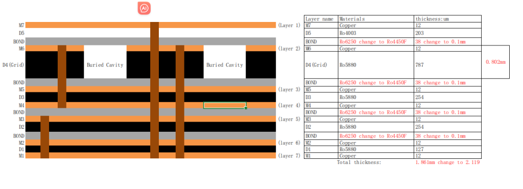
Die Form, Größe, und die Platzierung des Hohlraums sind entscheidend für die Optimierung der elektromagnetischen Eigenschaften und der Leistung der Antenne.
Auswahl der richtigen Leiterplattenmaterialien, die einen geringen dielektrischen Verlust bieten, hohe Wärmeleitfähigkeit, und eine stabile Leistung über alle Frequenzen hinweg ist unerlässlich.
Für die Minimierung von Signalreflexionen und -verlusten ist die Gewährleistung einer ordnungsgemäßen Impedanzanpassung zwischen der Antenne und dem Rest der Schaltung von entscheidender Bedeutung.
Um die durch die Hochfrequenzsignale erzeugte Wärme abzuleiten, müssen wirksame Wärmemanagementtechniken implementiert werden.
Um elektromagnetische Störungen zu verhindern, sind geeignete Abschirmtechniken erforderlich (EMI) und sorgen für eine saubere Signalübertragung.
Die Einhaltung enger Fertigungstoleranzen ist entscheidend für die Gewährleistung gleichbleibender Leistung und Zuverlässigkeit.
Materialien, die in Antennenhohlraum-Leiterplatten verwendet werden
Bei der Herstellung von Antennenhohlraum-Leiterplatten werden üblicherweise mehrere Materialien verwendet:
Materialien wie Rogers RT/duroid, RO4000, Die Serien RO3000 und RO3000 bieten einen geringen dielektrischen Verlust und eine stabile Leistung bei hohen Frequenzen.
Diese Materialien bieten hervorragende thermische und elektrische Eigenschaften, Dadurch sind sie für Hochfrequenzanwendungen geeignet.
Aufgrund seiner hervorragenden elektrischen Leitfähigkeit wird Kupfer für Leiterbahnen und Hohlraumwände verwendet.
TIMs, wie Wärmeleitpaste oder Wärmeleitpads, werden verwendet, um die Wärmeübertragung zwischen Komponenten und Kühllösungen zu verbessern.
Leitfähige Materialien, wie Kupfer oder Aluminium, dienen der Abschirmung zur Vermeidung elektromagnetischer Störungen.
Herstellungsprozess von Antennenhohlraum-Leiterplatten
Der Herstellungsprozess von Antennenhohlraum-Leiterplatten umfasst mehrere präzise Schritte:
Hochfrequenzlaminate und andere Materialien werden aufbereitet und zu Platten oder Folien verarbeitet.
Durch präzise Bearbeitungs- oder Ätztechniken werden Hohlräume innerhalb der Leiterplattenschichten erzeugt.
Die Schichten der Leiterplatte, einschließlich des Hohlraums, werden je nach Design gestapelt, unter sorgfältiger Berücksichtigung der Platzierung dielektrischer Materialien und Leiterbahnen.
Durchkontaktierungen werden gebohrt und plattiert, um vertikale elektrische Verbindungen zwischen verschiedenen Schichten und dem Hohlraum herzustellen.
Komponenten, inklusive der Antenne, werden mittels automatisierter Oberflächenmontagetechnologie auf der Leiterplatte montiert (SMT) Prozesse.
Kühlkörper, Kühlventilatoren, und thermische Schnittstellenmaterialien sind integriert, um ein effektives Wärmemanagement zu gewährleisten.
Um elektromagnetische Störungen zu verhindern und eine saubere Signalübertragung zu gewährleisten, werden Abschirmmaterialien verwendet.
Die zusammengebauten Platinen werden strengen Tests und Inspektionen unterzogen, um sicherzustellen, dass sie die erforderlichen Spezifikationen für die elektrische Leistung erfüllen, Signalintegrität, und Zuverlässigkeit.
Die getesteten und validierten Platinen werden in ihre endgültige Form zusammengebaut, verpackt, und für den Vertrieb vorbereitet.
Anwendungen von Antennenhohlraum-Leiterplatten
Antennenhohlraum-Leiterplatten werden in einer Vielzahl von Hochfrequenzanwendungen eingesetzt:
Diese Leiterplatten werden in Basisstationen verwendet, Antennen, und andere Kommunikationsgeräte, bei denen die Übertragung hochfrequenter Signale von entscheidender Bedeutung ist.
Antennenhohlraum-Leiterplatten sind in Radarsystemen unverzichtbar, Satellitenkommunikation, und Militärelektronik, wo Zuverlässigkeit und Leistung entscheidend sind.
Diese PCBs werden in medizinischen Bildgebungs- und Diagnosegeräten verwendet, die mit hohen Frequenzen arbeiten, eine präzise und zuverlässige Signalübertragung erfordern.
Antennenhohlraum-Leiterplatten werden in modernen Fahrerassistenzsystemen eingesetzt (Adas), Fahrzeug-zu-Alles (V2X) Kommunikation, und Radarsysteme.
Diese Leiterplatten werden in industriellen Sensoren verwendet, Automatisierungssysteme, und andere industrielle Hochfrequenzanwendungen.
Vorteile von Antennenhohlraum-Leiterplatten
PCBs mit Antennenhohlraum bieten mehrere Vorteile:
Die Hohlraumstruktur minimiert Signalverluste und Störungen, Verbesserung der Signalstärke und -klarheit.
Die Integration von Antennen in die Leiterplatte ermöglicht kompaktere Designs, Platzersparnis und Reduzierung der Gesamtgröße des Geräts.
Die kontrollierte Umgebung des Hohlraums schützt die Antenne vor Umwelteinflüssen, Verbesserung der Zuverlässigkeit und Langlebigkeit.
Diese Leiterplatten sind für den effizienten Betrieb bei hohen Frequenzen ausgelegt, Dadurch sind sie für HF- und Mikrowellenanwendungen geeignet.
Antennenhohlraum-Leiterplatten können an spezifische Anforderungen angepasst werden, inklusive Frequenzbereich, Krafthandhabung, und Umweltbedingungen.
FAQ
Was sind die Hauptvorteile der Verwendung von Antennenhohlraum-Leiterplatten??
Zu den Hauptvorteilen gehört eine verbesserte Signalleistung, kompaktes Design, verbesserte Zuverlässigkeit, Hochfrequenzfähigkeit, und Anpassbarkeit. Diese Vorteile machen Antennenhohlraum-Leiterplatten ideal für Hochfrequenz- und Hochleistungsanwendungen.
Welche Materialien werden üblicherweise in Antennenhohlraum-Leiterplatten verwendet??
Zu den gängigen Materialien gehören Hochfrequenzlaminate wie Rogers RT/Duroid, RO4000, und RO3000-Serie, Keramikgefülltes PTFE, Kupfer für Leiterbahnen und Hohlraumwände, Wärmeschnittstellenmaterialien (TIMs), und Abschirmmaterialien wie Kupfer oder Aluminium.
Wie gewährleistet das Design einer Antennenhohlraum-Leiterplatte eine hohe Leistung??
Das Design gewährleistet eine hohe Leistung durch die Optimierung des Hohlraumdesigns, Auswahl geeigneter Materialien, Gewährleistung einer ordnungsgemäßen Impedanzanpassung, Implementierung eines effektiven Wärmemanagements, Anwendung geeigneter Abschirmtechniken, und Einhaltung enger Fertigungstoleranzen.
Was sind die häufigsten Anwendungen von Antennenhohlraum-Leiterplatten??
Zu den häufigsten Anwendungen gehört die Telekommunikation (Basisstationen, Antennen), Luft- und Raumfahrt und Verteidigung (Radarsysteme, Satellitenkommunikation), Medizinprodukte (medizinische Bildgebung, Diagnostik), Automobilelektronik (Adas, V2X-Kommunikation), und industrielle Anwendungen (Sensoren, Automatisierungssysteme). Diese Leiterplatten werden in Systemen eingesetzt, die Hochfrequenzleistung und zuverlässige Signalübertragung erfordern.