CO.,LTD")
Hohlräume PCB -Herstellung, Offene Hohlraum-PCBs benötigen einen Tiefenausschnitt.
Multilayer -Leiterplatte mit Hohlräumen. Wir haben viele Hohlräume auf der leeren gedruckten Leiterplatte gemacht. Gute Qualität, Schnelle Lieferung, und günstigerer Preis. Unser PCB -Firma hat produziert Hohlraumkreis aus 4 Schicht zu 50 Lagen. Über die Hohlraumschaltmaterialien. Wenn Sie die PCB nur mit FR4 -Kernmaterialien benötigen. Wir werden sie in kurzer Kurve beenden. z.B: 4 Schicht zu 8 Schichthöhlenplatten. Wir werden sie beenden 10 Zu 15 Tage. aus 10 Schicht zu 20 Lagen Hohlraumbretter. Wir brauchen herum 15 Zu 20 Tage.
Die Hohlraumplatten mit besonderen Leitermaterialien. z.B: Hochleistungsschaltungsmaterialien, Niedrige Verluste FR4 Schaltungsmaterialien, Hochgeschwindigkeitsschaltungsmaterialien, Hochfrequenzschaltungsmaterialien. Die Vorlaufzeit wird etwas lang sein. Vielleicht brauchen 15 Zu 30 Tage. Bevor Sie uns die Gerber -Dateien senden. Wenn Sie Fragen haben. Bitte erkundigen Sie sich bei unserem Ingenieurteam. Über die PCB -Materialien. Wir haben viele spezielle Schaltungsmaterialien in unserem Lagerhaus. Einige sind sehr teuer. Einige sind billiger. Wenn Sie den Standard -FR4 -Kern verwenden, um die Hohlräume zu machen. Der Preis wird billiger sein. Wenn Sie verwenden Hochgeschwindigkeits- oder Hochfrequenzkern. Der PCB -Preis wird teuer sein. Materialien sind nicht gleich. Also. Der Preis wird nicht dasselbe sein.
DerHohlraum-PCB-Technologien. Ja. Wir können die Hohlraumplatten mit vielen fortschrittlichen Technologien herstellen. Beispiel: Wir können die Hohlraumplatine mit vergrabenen und blinden Vias herstellen. Bitte achten Sie darauf, es zu wissen. im Hohlraumbereich. Es gibt einige vergrabene oder blinde Vias-Löcher. Ich meine. Die Durchgangslöcher werden im Hohlraumbereich aus dem Kupfer herausragen.
Über die Materialien Dielektrika. wenn Sie brauchen. Wir können die Hohlraumplatine aus vielen verschiedenen dielektrischen Materialien herstellen. wie: Rogers-Dielektrika VS FR4-Dielektrika, Oder, Rogers-Dielektrika VS. Isola-Dielektrika, Oder M7, M4, M6-Dielektrika, und andereHochleistung, Verlustarme FR4-Dielektrika. Sag es uns einfach. Welche Arten von Dielektrika benötigen Sie bitte?? Sag es uns bitte. wir können es produzieren. und gute Arbeit leisten.
Über andere Cavity-PCB-Produktionstechnologien. wie: Impedanzkontrolle. wir können es tun +/-5%, Hinterbohren, Bohren und Fräsen mit kontrollierter Tiefe, Starr-Flex & Flexible Schaltkreise, und andere. Unser Unternehmen hat viele militärische PCB-Produkte hergestellt, Luftfahrt-PCB, Militärische Kommunikationsplatine, Industrielles PCB-Produkt, und viele Produkte in anderen Bereichen.
Was ist eine Hohlraum -PCB?
Eine Hohlraum -PCB, Auch als Hohlraum-Board oder Hohlraum-Junggesellschaften bezeichnet, ist eine Art gedruckter Leiterplatte mit einem eingebrauchten Bereich oder Hohlraum, der in einem oder beiden Seiten bearbeitet wurde. Dieser vertiefte Bereich kann je nach den spezifischen Anforderungen der Anwendung in der Tiefe und Form variieren.
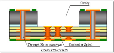
Bau von Hohlraum-Leiterplatten: Hohlraum -PCBs werden typischerweise unter Verwendung herkömmlicher PCB -Herstellungstechniken konstruiert, mit dem zusätzlichen Schritt des Mahlens oder des Ausleitens eines Hohlraums auf einem oder beiden Seiten des Boards. Dieser Hohlraum kann mit CNC zu präzisen Abmessungen bearbeitet werden (Computer-Numerische Steuerung) Maschinen oder andere fortschrittliche Fertigungsgeräte. Das verbleibende PCB -Substrat bildet die Basis oder die Wände des Hohlraums, Bereitstellung einer strukturellen Integrität für den Vorstand.
Anwendungen von Hohlraum-Leiterplatten: Hohlraum -PCBs finden Anwendungen in verschiedenen Branchen, in denen spezielle Designs erforderlich sind, um bestimmte Leistungskriterien zu erfüllen. Einige gemeinsame Anwendungen umfassen:
- Antennensysteme: Hohlraum -PCBs werden in RF häufig verwendet (Funkfrequenz) und Mikrowellenanwendungen, vor allem in Antennensystemen. Der Hohlraum fungiert als Schutzschild, Reduzierung der elektromagnetischen Störungen (EMI) und Verbesserung der Antennenleistung.
- Hochfrequenzkreise: Aufgrund ihrer überlegenen Signalintegritätseigenschaften, Hohlraum-PCBs werden in Hochfrequenzschaltungen wie Radarsystemen verwendet, Telekommunikationsgeräte, und drahtlose Geräte.
- Luft- und Raumfahrt und Verteidigung: Die Luft- und Raumfahrt- und Verteidigungsindustrie nutzen Hohlraum -PCBs in kritischen Systemen, wo Zuverlässigkeit, Haltbarkeit, und Leistung sind von größter Bedeutung. Diese Boards werden häufig in Avionik eingesetzt, Radarsysteme, und Raketenleitsysteme.
- Medizinprodukte: In medizinischer Elektronik, insbesondere in diagnostischen Geräten und Bildgebungsgeräten, Hohlraum -PCBs bieten eine verstärkte Signalklarheit und Rauschreduzierung, Beitrag zu genaueren Lesungen und Diagnosen.
Vorteile von Hohlraum-PCBs: Die Nutzung von Hohlraum -PCBs bietet mehrere Vorteile, einschließlich:
- Verbesserte Signalintegrität: Das Hohlraumdesign reduziert elektromagnetische Störungen, Gewährleistung der saubereren Signalübertragung und -empfang, vor allem in hochfrequenten Anwendungen.
- Verbessertes thermisches Management: Hohlraum -PCBs ermöglichen eine effizientere Wärmeableitung, entscheidend für elektronische Komponenten, die in anspruchsvollen Umgebungen arbeiten.
- Raumoptimierung: Durch die Integration von Komponenten innerhalb der Kavität, Cavity-Leiterplatten ermöglichen kompakte und leichte Designs, Ideal für platzbeschränkte Anwendungen wie tragbare Elektronik und Luft- und Raumfahrtsysteme.
Überlegungen zum Hohlraum -PCB -Design: Während Hohlraum -PCB zahlreiche Vorteile bietet, Bestimmte Überlegungen müssen während des Entwurfs- und Herstellungsprozesses berücksichtigt werden:
- Kosten: Die Bearbeitung von Hohlräumen trägt zu den Herstellungskosten von PCBs bei, Hohlraumtafeln im Vergleich zu Standard -PCBs teurer machen.
- Mechanische Stabilität: Auf die mechanische Integrität von Hohlraum -PCBs muss sorgfältig Aufmerksamkeit geschenkt werden, um sicherzustellen, dass sie Umweltbelastungen standhalten und die strukturelle Stabilität aufrechterhalten können.
Abschluss: Hohlraum -PCBs stellen eine spezialisierte Lösung dar, die auf anspruchsvolle Anwendungen zugeschnitten ist, die eine hohe Leistung erfordern, Zuverlässigkeit, und Signalintegrität. Mit ihrem einzigartigen Design und Konstruktion, Diese Boards spielen eine wichtige Rolle in verschiedenen Branchen, einschließlich Telekommunikation, Luft- und Raumfahrt, Verteidigung, und medizinische Elektronik, Förderung von Innovation und Fortschritt in elektronischen Systemen.
So entwerfen Sie eine Leiterplatte: Eine Schritt-für-Schritt-Anleitung?
Einführung: Entwurf einer Leiterplatte (Leiterplatte) ist ein entscheidender Schritt bei der Entwicklung elektronischer Geräte. Egal, ob Sie ein erfahrener Ingenieur oder ein Anfänger -Enthusiast sind, Das Verständnis der Grundlagen des PCB -Designs ist unerlässlich. Dieser Leitfaden führt Sie durch den Prozess des Entwerfens einer PCB, von der Konzeptualisierung bis zur Herstellung, Hervorhebung wichtiger Schritte und Überlegungen auf dem Weg.
Schritt 1: Definieren Sie die Anforderungen, bevor Sie in den Entwurfsprozess eintauchen, Definieren Sie die Anforderungen Ihrer PCB klar. Betrachten Sie Faktoren wie die Größenbeschränkungen, elektrische Spezifikationen, Platzierung der Komponenten, und Umgebungsbedingungen, unter denen die PCB betrieben wird.
Schritt 2: Schematisches Design Erstellen Sie ein schematisches Diagramm Ihrer Schaltung mit EDA (Elektronische Designautomatisierung) Software wie Altium -Designer, Adler, oder Kicad. Dieser Schaltplan dient als Blaupause für die Verbindungen zwischen Komponenten und definiert das elektrische Verhalten der Schaltung.
Schritt 3: Auswahl und Platzierung der Komponenten Wählen Sie die für Ihren Schaltkreis erforderlichen Komponenten aus, basierend auf der Funktionalität, Verfügbarkeit, und Kosten. Einmal ausgewählt, Platzieren Sie die Komponenten gemäß dem Schaltplan auf dem PCB-Layout. Berücksichtigen Sie Faktoren wie die Signalführung, Wärmemanagement, und einfache Montage während der Komponentenplatzierung.
Schritt 4: PCB -Layout mit den platzierten Komponenten, Fahren Sie mit der Layoutstufe der PCB fort. Ordnen Sie die Komponenten auf der Leiterplatte an, um die Signalintegrität zu optimieren, Störungen minimieren, und sorgen für eine effiziente Streckenführung. Achten Sie auf Faktoren wie die Spurlänge, Impedanzkontrolle, und Signalrückwege während der Layoutgestaltung.
Schritt 5: Routing Verbinden Sie die Komponenten auf dem PCB-Layout, indem Sie Leiterbahnen zwischen ihnen verlegen. Befolgen Sie die Best Practices für das Trace-Routing, wie zum Beispiel die Beibehaltung konsistenter Leiterbahnbreiten, Vermeiden Sie scharfe Ecken, und Minimierung des Signalübersprechens. Verwenden Sie Erdungs- und Stromebenen, um eine stabile Spannungsverteilung zu gewährleisten und elektromagnetische Störungen zu reduzieren.
Schritt 6: Design-Regelprüfung (Demokratische Republik Kongo) Führen Sie eine Konstruktionsregelprüfung durch, um sicherzustellen, dass Ihr PCB -Design den Fertigungsbeschränkungen und Branchenstandards entspricht. Dies beinhaltet die Überprüfung auf Verstöße gegen die Freigabe, minimale Leiterbahnbreiten, und die richtigen Padgrößen. Beheben Sie alle während des DRC-Prozesses festgestellten Fehler oder Warnungen.
Schritt 7: Konstruktionsüberprüfung, bevor Sie zur Herstellung fortfahren, Überprüfen Sie die Funktionalität und Integrität Ihres PCB-Designs durch Simulation und Tests. Verwenden Sie Gewürz (Simulationsprogramm mit integrierter Schaltung Schwerpunkt) Software zur Simulation des Schaltungsverhaltens und zur Validierung der Leistung gegen Designspezifikationen. Erstellen Sie Prototypen und testen Sie die Leiterplatte, um etwaige Probleme zu identifizieren und notwendige Anpassungen vorzunehmen.
Schritt 8: Generieren Sie Herstellungsdateien, sobald Ihr PCB -Design fertiggestellt und verifiziert ist, Generieren Sie die für die Fertigung erforderlichen Fertigungsdateien. Zu diesen Dateien gehören typischerweise Gerber-Dateien für PCB-Grafiken, Bohrfeilen für die Lochplatzierung, und eine Stückliste (Stückliste) detaillierte Komponentenspezifikationen. Überprüfen Sie die Fertigungsdateien, um die Genauigkeit zu gewährleisten, bevor Sie sie an den PCB -Hersteller senden.
Schritt 9: Fertigung und Montage Senden Sie die Fertigungsdateien zur Produktion an eine PCB-Fertigungsanlage. Wählen Sie einen seriösen Hersteller aus, der Qualitätsfabrik -Dienstleistungen anbietet und Ihre Spezifikationen festhält. Nach Erhalt der gefertigten Leiterplatten, Fahren Sie mit der Komponentenmontage und dem Löten gemäß der Stückliste und Montageanleitung fort.
Abschluss: Der Entwurf einer Leiterplatte erfordert eine sorgfältige Planung, Aufmerksamkeit fürs Detail, und Einhaltung bewährter Praktiken. Durch die folgende Schritt-für-Schritt-Anleitung, Sie können eine gut gestaltete Leiterplatte erstellen, die Ihren Projektanforderungen entspricht und in der vorgesehenen Anwendung zuverlässig funktioniert. Verfeinern Sie kontinuierlich Ihre Designfähigkeiten und bleiben Sie über Fortschritte in der PCB-Technologie auf dem Laufenden, um immer komplexere Designherausforderungen souverän zu meistern.
Wie man herstellen Hohlraumplatine?
Ein umfassender Leitfaden für PCBs der Herstellung von Hohlraum: Einführung: Hohlraum-Leiterplatten, bekannt für ihr spezielles Design mit vertieften Bereichen, Bieten Sie eine verbesserte Leistung in verschiedenen elektronischen Anwendungen an. Die Herstellung dieser Boards erfordert Präzision und Fachwissen, um optimale Funktionen zu erreichen. Dieser Leitfaden bietet einen detaillierten Überblick über den Herstellungsprozess für Hohlraum -PCBs, Abdeckung wichtiger Schritte und Überlegungen.
Schritt 1: Konstruktion und Technik Der Herstellungsprozess für Hohlraum -PCBs beginnt mit umfassendes Design und Engineering. Ingenieure planen das Layout sorgfältig, Berücksichtigung von Faktoren wie Hohlraumabmessungen, Materialauswahl, und elektrische Anforderungen. Spezialer CAD (Computergestütztes Design) Software wird verwendet, um präzise Designs zu erstellen, die den Spezifikationen der beabsichtigten Anwendung entsprechen.
Schritt 2: Die Auswahl der Materialauswahl für geeignete Materialien ist entscheidend für die CAVity -PCB -Herstellung. Hochwertige Substratmaterialien, wie FR-4 (Flammschutzmittel 4), PTFE (Polytetrafluorethylen), oder Keramik, werden üblicherweise für ihre thermische Stabilität verwendet, dielektrische Eigenschaften, und mechanische Festigkeit. Zusätzlich, Leitfähigkeitsmaterialien für Schaltungsspuren und Komponentenpolster werden basierend auf der Leitfähigkeit ausgewählt, Korrosionsbeständigkeit, und Kompatibilität mit dem Herstellungsprozess.
Schritt 3: Hohlraumbearbeitung Das definierende Merkmal von Hohlraum -PCBs ist der in die Platine eingerichtete Umtauchbereich. Dieser Schritt umfasst Präzisionsbearbeitung mit CNC (Computer-Numerische Steuerung) Ausrüstung oder spezialisierte Fräsmaschinen. Die Hohlraumabmessungen müssen genau mit den Entwurfsspezifikationen übereinstimmen, um die ordnungsgemäße Komponentenanpassung und Funktionalität sicherzustellen. Sorgfältige Aufmerksamkeit wird zur Aufrechterhaltung der Gleichmäßigkeit und der Glätte der Hohlraumwände gelegt, um strukturelle Schwächen oder Signalstörungen zu verhindern.
Schritt 4: Schichtausrichtung und Bindung in mehrschichtigen Hohlraum-PCBs, Einzelne Schichten sind ausgerichtet und miteinander verbunden, um eine einheitliche Struktur zu bilden. Die Ausrichtung ist von entscheidender Bedeutung, um eine ordnungsgemäße Registrierung von leitenden Spuren und VIAS über die Schichten zu gewährleisten. Verschiedene Bindungstechniken, wie Laminierung oder Klebstoffbindung, werden basierend auf den Substratmaterialien und den Entwurfsanforderungen verwendet. Die richtige Bindung sorgt für die strukturelle Integrität und die elektrische Kontinuität im gesamten PCB.
Schritt 5: Schaltungsstrukturierung und Ätzen, sobald die Substratschichten verbunden sind, Die Schaltungsmuster werden auf die PCB -Oberfläche übertragen. Dies erfolgt normalerweise mit einer photoresistischen Maske und einem Ätzprozess. Der Photoresist wird auf das Substrat angewendet, UV -Licht durch eine Fotomaske ausgesetzt, und entwickelt, um das gewünschte Schaltungsmuster aufzudecken. Anschließend werden die freigelegten Stellen mit chemischen Lösungen weggeätzt, hinterlassen die leitenden Spuren und Komponentenpolster hinterlassen.
Schritt 6: Plattier- und Oberflächen -Finishing -leitende Oberflächen der Leiterplatte, einschließlich Schaltungsspuren und Komponentenpolster, werden mit Metall plattiert, um die Leitfähigkeit und Haltbarkeit zu verbessern. Gemeinsame Beschichtungsmetalle umfassen Kupfer, Nickel, und Gold. Oberflächen -Finishing -Techniken, wie Hasl (Heißluft-Lotnivellierung), ZUSTIMMEN (Chemisches Nickel-Immersionsgold), oder OSP (Organisches Lötbarkeitskonservierungsmittel), werden angewendet, um exponierte Oberflächen vor Oxidation zu schützen und die Lötlichkeit während der Montage zu erleichtern.
Schritt 7: Qualitätssicherung und Tests während des gesamten Herstellungsprozesses, Qualitätssicherungsmaßnahmen werden implementiert, um die Integrität und Funktionalität der Hohlraum -PCBs sicherzustellen. Visuelle Inspektion, Dimensionsmessungen, elektrische Tests, und thermische Analysen werden in verschiedenen Stadien durchgeführt, um Mängel oder Abweichungen von den Spezifikationen zu erkennen und zu beheben. Umfassende Tests bestätigen die Leistung und Zuverlässigkeit der fertigen PCB, bevor sie für die Montage und Integration in elektronische Systeme freigesetzt werden.
Abschluss: PCBs der Fertigungshöhle erfordert eine Kombination aus fortschrittlicher Technologie, Präzisionstechnik, und strenge Qualitätskontrollmaßnahmen. Durch Befolgen des umrissenen Prozess, Hersteller können hochwertige Hohlraum-PCB produzieren, die den anspruchsvollen Anforderungen moderner elektronischer Anwendungen entsprechen. Kontinuierliche Innovation und Verfeinerung der Fertigungspraktiken verbessern die Leistung und Vielseitigkeit von Hohlraum -PCBs in verschiedenen Branchen weiter.
Wir können viele Arten von Hohlräumen in hochschichtigen Leiterplatten herstellen. Wenn Sie irgendwelche Fragen haben, Nehmen Sie gerne Kontakt mit uns aufinfo@alcantapcb.com , Wir helfen Ihnen gerne weiter.