CO.,LTD")
Hersteller von Hohlraumsubstrat-Leiterplatten. Hochgeschwindigkeits- und Hochfrequenz-Materialhohlraum Verpackungssubstrat und Herstellung von Cavity-Leiterplatten. Fortschrittliche Produktionstechnologie.
Hohlraumsubstrat Leiterplatten, im Chinesischen als solches bekannt, stellen einen bedeutenden Fortschritt in der Leiterplattentechnik dar. Sie verfügen über spezielle Hohlräume in ihrem Design, Bietet eine optimale Montageumgebung für elektronische Komponenten. Diese einzigartige Struktur verbessert nicht nur die elektrische Leistung durch die Minimierung von Problemen wie Signalinterferenzen und Kreuzkopplung, sondern verbessert auch die Wärmemanagementfähigkeiten. Folglich, Diese Leiterplatten sind entscheidende Komponenten im modernen elektronischen Gerätedesign.
In modernen elektronischen Geräten, Temperaturmanagement ist entscheidend geworden. Hohlraumsubstrat-Leiterplatten bieten durch ihr spezielles Hohlraumdesign hervorragende Wärmemanagementfähigkeiten. Diese Struktur trägt nicht nur zur Wärmeableitung bei, sondern isoliert auch wirksam Wärmequellen und verhindert eine ungleichmäßige Temperaturverteilung auf der Leiterplatte. daher, Hohlraumsubstrat-Leiterplatten eignen sich ideal für den zuverlässigen Betrieb elektronischer Komponenten in Umgebungen mit hohen Temperaturen.
Das Aufkommen von Hohlraumsubstrat-Leiterplatten markiert den Trend in der Elektrotechnik hin zu höherer Leistung und kleinerer Größe. Dieses fortschrittliche Substratdesign erfüllt nicht nur die hohen Leistungs- und Dichteanforderungen moderner elektronischer Geräte, sondern bietet Ingenieuren auch innovativere Möglichkeiten. Es ist sehr anpassungsfähig und kann verschiedene Anwendungsszenarien nutzen, Dadurch werden kontinuierliche Innovationen im gesamten Bereich der Elektrotechnik gefördert.
Hohlraumsubstrat-Leiterplatten, als aufstrebende Wahl für die Montage elektronischer Komponenten, stellen nicht nur einen wichtigen Fortschritt in der Leiterplattentechnik dar, sondern weisen auch eine hervorragende elektrische Leistung und ein hervorragendes Wärmemanagement auf. Das Design seines speziellen Hohlraums bietet eine ideale Montageplattform für moderne elektronische Geräte, Dies bietet Ingenieuren mehr Innovationsmöglichkeiten. Während sich diese Technologie weiterentwickelt, Wir können damit rechnen, Zeuge einer neuen Ära des Wohlstands im Elektronikdesign zu werden.
Welche Arten von Hohlraumsubstrat-Leiterplatten gibt es??
In der modernen Leiterplattentechnik, Hohlraumsubstrat-Leiterplatten zeichnen sich aufgrund ihrer Anpassungsfähigkeit als herausragende Technologie aus, Es erregt große Aufmerksamkeit in Elektronikdesign- und Fertigungskreisen. Ziel dieses Artikels ist es, verschiedene Arten von Hohlraumsubstrat-PCBs zu untersuchen, mit besonderem Schwerpunkt auf Schlüsselvarianten wie High-Density-Interconnect (HDI) und Starr-Flex-Kombinationen. Durch die Untersuchung ihrer unterschiedlichen Merkmale in Designvoraussetzungen und Nutzungsszenarien, Wir decken die vielfältigen Einsatzmöglichkeiten und Anforderungen dieser innovativen Leiterplattentypen auf.
HDI (Hochdichte Verbindung) Hohlraumsubstrat-Leiterplatten
Sein Hauptmerkmal ist seine hochintegrierte Verbindungsstruktur, Dadurch können mehr elektronische Komponenten auf begrenztem Raum untergebracht werden. Dadurch können HDI-Hohlraumsubstrat-Leiterplatten eine hervorragende Leistung in kleinen elektronischen Geräten erzielen, Bereitstellung einer idealen Lösung für mobile Geräte, Smart Wearables und andere Bereiche.
Starrflexible Hohlraumsubstrat-Leiterplatten
Leiterplatten mit starr-flexiblem Hohlraumsubstrat kombinieren starre und flexible Materialien, Bietet Designern Vielseitigkeit bei der Erstellung von Platinen, die in bestimmten Abschnitten die Steifigkeit beibehalten und in anderen Abschnitten Flexibilität ermöglichen. Diese Leiterplatten finden umfangreiche Anwendung in elektronischen Geräten wie faltbaren Mobiltelefonen und Wearables, die Biege- und Faltfähigkeiten erfordern.
Vielfalt an Hohlraumsubstrat-Leiterplatten
Zusätzlich zu den beiden oben genannten Haupttypen, Die Hohlraumsubstrat-PCB-Technologie hat auch viele andere Varianten hervorgebracht, um unterschiedlichen Designanforderungen und Anwendungsszenarien gerecht zu werden. Dazu können kundenspezifische Hohlraumsubstrat-Leiterplatten mit speziellen Hohlraumstrukturen für bestimmte Industrieanwendungen oder elektronische Geräte in extremen Umgebungen gehören.
Verschiedene Arten von Hohlraumsubstrat-Leiterplatten werden mit unterschiedlichen Designmerkmalen maßgeschneidert, um den spezifischen Anwendungsanforderungen gerecht zu werden. Zum Beispiel, HDI-Hohlraumsubstrat-Leiterplatten sind ideal für kompakte mobile Geräte, wohingegen Starrflex-Hohlraumsubstrat-Leiterplatten für Elektronikanwendungen geeignet sind, die flexible Designs erfordern. Die Vielfalt dieser Leiterplatten spiegelt die Vielfalt der eingesetzten innovativen Fertigungstechnologien wider, wie Präzisionslaminierung und Hohlraumbearbeitung, um die Einhaltung von Design- und Leistungsvorgaben zu gewährleisten.
Die Vielfalt der Cavity-Substrat-PCB-Typen spiegelt die kontinuierliche Innovation im elektronischen Design und in der Fertigung wider. Ganz gleich, ob es darum geht, Anforderungen an hochdichte Verbindungen zu erfüllen oder starr-flexible Designs zu erreichen, Die Cavity-Substrat-PCB-Technologie spielt eine Schlüsselrolle bei der Förderung von Durchbrüchen in der modernen Elektronik. Diese Vielfalt bietet Designern mehr Möglichkeiten, Dadurch können sie sich besser an veränderte Marktbedürfnisse anpassen.
Was sind die Vorteile der Verwendung von Cavity Substrate PCB??
Das Aufkommen von Hohlraumsubstrat-Leiterplatten markiert einen bedeutenden Fortschritt im modernen Elektronikdesign, Bietet unübertroffene Vorteile in der elektrischen Funktionalität, Größenminimierung, und Wärmeableitung. Diese Leiterplatten nutzen fortschrittliche Methoden wie hochdichte Verbindungen (HDI), Bereitstellung beschleunigter Signalübertragungsraten und minimierter Verzerrungen. Folglich, Sie sind für hochfrequente und leistungsstarke Aufgaben sehr gefragt, festigen ihre Position als erste Wahl im Bereich Elektronikdesign.
Darüber hinaus, Hohlraumsubstrat-Leiterplatten ermöglichen eine erhebliche Miniaturisierung durch innovative Herstellungsmethoden und Materialien, Bewältigung der Herausforderung der Größenreduzierung, vor der Konstrukteure stehen. Dies schafft nicht nur Platz für das Gerätedesign, sondern ermöglicht auch eine flexiblere Anpassung elektronischer Produkte an vielfältige Anwendungsszenarien in immer kompakteren Formfaktoren. Gesamt, Die Einführung von Hohlraumsubstrat-Leiterplatten hat die Elektroniktechnik revolutioniert, bietet unübertroffene Vorteile in der elektrischen Leistung, Größeneffizienz, und Wärmeregulierung.
Hohlraumsubstrat-Leiterplatten verteilen und leiten Wärme durch ihre einzigartige Struktur effizienter. Dies ist entscheidend, um eine Überhitzung elektronischer Komponenten zu vermeiden und die Gerätestabilität zu verbessern. Dieser Vorteil macht Hohlraumsubstrat-Leiterplatten zu hervorragenden Hochleistungsplatinen, elektronische Anwendungen mit hoher Dichte.
Designs mit Hohlraumsubstrat-Leiterplatten bieten in vielerlei Hinsicht erhebliche Vorteile. Dies ist nicht nur eine technische Verbesserung, sondern auch, um den wachsenden Anforderungen moderner elektronischer Geräte gerecht zu werden. Die Verbesserung der elektrischen Leistung gewährleistet die Zuverlässigkeit der Datenübertragung, Die Möglichkeit zur Miniaturisierung macht das Gerätedesign flexibler, und ein hervorragendes Wärmemanagement sorgen für einen langfristig effizienten Betrieb der Geräte.
Gesamt, Hohlraumsubstrat-Leiterplatten, als zukunftsweisende Technologie, bietet mit seiner hervorragenden elektrischen Leistung neue Möglichkeiten für die Entwicklung und Herstellung fortschrittlicher elektronischer Geräte, Miniaturisierung und Wärmemanagement. Ob im Bereich Kommunikation, medizinische Geräte oder industrielle Anwendungen, Hohlraumsubstrat-Leiterplatten werden nach und nach zur ersten Wahl für Elektronikdesigner, treibt die kontinuierliche Weiterentwicklung der Elektrotechnik voran.
Warum Cavity Substrate PCB anstelle anderer Platinen wählen??
In der dynamischen Landschaft der Elektronik, Hohlraumsubstrat-Leiterplatten haben sich aufgrund ihrer außergewöhnlichen Leistung als Vorreiter im elektronischen Design und in der Fertigung etabliert, effiziente Raumnutzung, und Kompatibilität mit fortschrittlichen Technologien. Diese Wahl gegenüber herkömmlichen Leiterplatten spiegelt die erheblichen Vorteile wider, die Hohlraumsubstrat-Leiterplatten in der sich schnell entwickelnden Industrie von heute bieten.
Hohlraumsubstrat-Leiterplatten übertreffen herkömmliche Leiterplatten in puncto Leistung bei weitem. Es nutzt fortschrittliche Materialien und Fertigungstechnologien, um durch eine spezielle Hohlraumstruktur eine hervorragende elektrische Leistung zu bieten. Im Vergleich zu herkömmlichen Leiterplatten, Hohlraumsubstrat-Leiterplatten können die Wärme effektiver verwalten und Störungen bei der Signalübertragung reduzieren, Dadurch wird eine stabilere und zuverlässigere elektronische Leistung erreicht.
Hohlraumsubstrat-Leiterplatten zeichnen sich durch ihr kompaktes Design und ihren hohen Integrationsgrad aus. Durch die Verwendung von hochdichten Verbindungen (HDI) Technologie, Dieses Substrat kann mehr elektronische Komponenten auf begrenztem Raum unterbringen, Dadurch wird eine Miniaturisierung und ein geringes Gewicht des Geräts erreicht. Diese hervorragende Raumausnutzung macht Hohlraumsubstrat-Leiterplatten ideal für kompakte Designs in modernen elektronischen Geräten.
Im heutigen sich schnell entwickelnden Technologiebereich, Hohlraumsubstrat-Leiterplatten haben sich als äußerst vielseitige Lösungen herausgestellt, mit bemerkenswerter technischer Anpassungsfähigkeit. Maßgeschneidert für verschiedene hochmoderne Anwendungen wie Hochfrequenzkommunikation, Hochgeschwindigkeitsdatenübertragung, und kompakte Bauformen, Diese Leiterplatten übertreffen herkömmliche Gegenstücke. Ihre überragende Flexibilität ermöglicht eine nahtlose Integration mit neuen Technologien, Gewährleistung müheloser Geräte-Upgrades auf der ganzen Linie.
Darüber hinaus, Hohlraumsubstrat-Leiterplatten zeichnen sich nicht nur durch Leistung und Platzausnutzung aus, sondern auch durch mehrschichtige Designs. Durch die Integration elektronischer Komponenten über verschiedene Ebenen hinweg, Diese Leiterplatten verwalten die Signalübertragung und Wärmeableitung effizient, Gewährleistung einer zuverlässigeren und stabileren Betriebsumgebung.
daher, Bei der Entscheidung für Hohlraumsubstrat-Leiterplatten gegenüber herkömmlichen Leiterplatten geht es nicht nur darum, einem Trend zu folgen, sondern darum, überlegene Leistungen zu erbringen, Hervorragende Raumausnutzung und Anpassung an fortschrittliche Technologie. Im elektronischen Design und in der Fertigung, Hohlraumsubstrat-Leiterplatten stellen zweifellos die Zukunft dar, Wir bieten starke Unterstützung für Innovationen und die Verwirklichung überlegener Leistungen.
Wie werden Hohlraumsubstrat-Leiterplatten hergestellt??
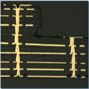
Hohlraumsubstrat-Leiterplatten stellen eine hochentwickelte Technologie im elektronischen Design und in der Fertigung dar, zeichnet sich durch aufwendige und präzise Produktionsprozesse aus. Dieser Artikel befasst sich mit den Herstellungstechniken von Hohlraumsubstrat-Leiterplatten, mit Schwerpunkt auf der Motherboard- und Substratproduktion. Es werden die wesentlichen Schritte erläutert, Materialien, und unterstreichen die entscheidende Rolle fortschrittlicher Technologie bei der Weiterentwicklung dieses Herstellungsprozesses.
Der subtraktive Prozess erreicht eine präzise Formgebung des Motherboards durch präzises Schneiden und Entfernen von unnötigem Material. Der additive Prozess baut eine komplexe Motherboard-Struktur auf, indem Materialien Schicht für Schicht hinzugefügt werden. Die Kombination dieser beiden Prozesse stellt sicher, dass Hohlraumsubstrat-Leiterplatten hochpräzise und anpassbar sind.
Fortschrittliche Materialien, beispielsweise solche mit hoher Wärmeleitfähigkeit und hochfesten Substraten, werden in großem Umfang bei der Herstellung von Hohlraumsubstrat-Leiterplatten eingesetzt, um die Leistung und Zuverlässigkeit der Schaltung zu verbessern. Gleichzeitig, Modernste Fertigungstechniken wie Laserschneiden und Präzisionsätzen garantieren die präzise Herstellung komplizierter Strukturen und Verkabelungen auf dem Motherboard, Schaffung einer soliden Grundlage für die effiziente Funktionalität elektronischer Geräte.
Strukturen zur Aufnahme und zum Schutz elektronischer Komponenten. Die hochdichte Verbindungstechnologie realisiert enge Verbindungen zwischen verschiedenen elektronischen Komponenten durch feine Linien und Durchgangslöcher, Verbesserung der Integration und Leistung von Schaltkreisen.
Bei der Substratherstellung von Hohlraumsubstrat-Leiterplatten, Die Materialauswahl ist entscheidend. Hochleistungsmaterialien wie FR-4 und Polyimid mit hervorragenden Isolationseigenschaften und Hochtemperaturstabilität werden häufig verwendet. Gleichzeitig wird die Zuverlässigkeit der Schaltung gewährleistet, Sie können auch den Arbeitsanforderungen in Umgebungen mit hohen Temperaturen effektiv standhalten, Dadurch sind Hohlraumsubstrat-Leiterplatten für verschiedene raue Anwendungsszenarien geeignet.
Diese gründliche Untersuchung der Motherboard- und Substratherstellung hat Licht auf den komplizierten Prozess geworfen, der bei der Herstellung von Cavity-Substrat-PCBs erforderlich ist. Es unterstreicht die zentrale Rolle, die fortschrittliche Materialien und Technologien in diesem Bereich spielen. Diese bahnbrechenden Fertigungstechniken bilden eine solide Grundlage für die Verbesserung der Leistung elektronischer Geräte und die Erweiterung ihres Anwendungsspektrums. Mit dem Aufkommen dieser neuen Ära bei Hohlraumsubstrat-Leiterplatten, Elektronikdesigner und -hersteller sind bereit, weitere Horizonte zu erkunden und neue Möglichkeiten zu erschließen.
Welche Anwendungen gibt es für Cavity Substrate PCB??
Hohlraumsubstrat-Leiterplatten stehen heute an der Spitze der Elektrotechnik, Aufgrund ihres außergewöhnlichen Designs und ihrer Anpassungsfähigkeit erweisen sie sich branchenübergreifend als unverzichtbar. Von der Luft- und Raumfahrt über Telekommunikation bis hin zu medizinischen Geräten, Diese fortschrittlichen Substrate werden häufig verwendet, Sie demonstrieren ihre Vielseitigkeit und ihre wesentliche Rolle bei innovativen Elektronikdesigns.
In der Luft- und Raumfahrt, Hohlraumsubstrat-Leiterplatten sind sowohl für Luft- als auch für Raumfahrzeuge von entscheidender Bedeutung. Ihre leichte Bauweise und die hochdichten Verbindungen machen sie perfekt für Avioniksysteme. Ihr umfangreicher Einsatz in der Navigation, Kommunikation, und Steuerungssysteme verbessern die Gesamtsystemleistung und -zuverlässigkeit erheblich.
In der sich schnell entwickelnden Kommunikationsbranche, Hohlraumsubstrat-Leiterplatten sind zum Kern moderner Kommunikationsgeräte geworden. Aufgrund seiner hochintegrierten Beschaffenheit spielt es eine Schlüsselrolle in drahtlosen Basisstationen, Kommunikationsnetzwerkausrüstung und Satellitenkommunikationssysteme. Diese Substrate ermöglichen Fortschritte in der Kommunikationstechnologie, indem sie eine überlegene Signalübertragungs- und Verarbeitungsleistung bieten.
Hohlraumsubstrat-Leiterplatten werden in verschiedenen Branchen wie der Herstellung medizinischer Geräte immer wichtiger, Industrielle Automatisierung, und Automobiltechnik. Diese Substrate, bekannt für ihre Anpassbarkeit und Zuverlässigkeit, erfüllen wichtige Funktionen in komplexen Geräten wie medizinischen Bildgebungsgeräten, Industrielle Steuerungssysteme, und Fahrzeugelektronik. Ihre Fähigkeit, hohen Temperaturen standzuhalten und eine hohe Dichte zu bieten, macht sie ideal für anspruchsvolle Umgebungen. Durch die Verbesserung der Leistung und Zuverlässigkeit elektronischer Geräte, Diese Substrate treiben Innovationen in verschiedenen Sektoren voran, Berücksichtigung einzigartiger Branchenanforderungen und Beschleunigung des technologischen Fortschritts.
Wo finden Sie Cavity-Substrat-PCB??
In der heutigen Elektrotechniklandschaft, Die Nachfrage nach Hochleistungs-Hohlraumsubstrat-Leiterplatten steigt. Diese Spezialkomponenten bieten überlegene Eigenschaften, die für moderne Design- und Herstellungsprozesse unerlässlich sind. Jedoch, Die Suche nach zuverlässigen und qualitativ hochwertigen Hohlraumsubstrat-Leiterplatten auf dem expansiven Markt kann für Ingenieure und Entscheidungsträger gleichermaßen eine große Herausforderung darstellen. Ziel dieses Artikels ist es, eine Anleitung zur effektiven Beschaffung dieser fortschrittlichen Tools für die elektronische Entwicklung zu geben, Es ermöglicht den Lesern, fundierte Entscheidungen für ihre Projekte zu treffen.
Fachkompetenz:Mit umfangreicher Berufserfahrung, Wir sind führend auf diesem Gebiet, umfassendes Verständnis der Design- und Herstellungsdetails von Hohlraumsubstrat-Leiterplatten, um verschiedene Projektanforderungen effektiv zu erfüllen.
Fortschrittliche Technologie:Wir setzen modernste Fertigungstechnologien ein, einschließlich High Density Interconnect (HDI), um die Leistung und Zuverlässigkeit unserer Hohlraumsubstrat-Leiterplatten auf ein optimales Niveau zu heben.
Qualitätssicherung:Unsere strengen Qualitätskontrollpraktiken erstrecken sich von der Rohstoffbeschaffung über die Produktion bis zur endgültigen Lieferung, Wir stellen sicher, dass jede Hohlraumsubstrat-Leiterplatte kompromisslosen Qualitätsstandards entspricht.
Anpassung:Wir bieten flexible Anpassungsdienste an, die auf die spezifischen Bedürfnisse unserer Kunden zugeschnitten sind, Gewährleistung einer nahtlosen Integration mit unterschiedlichen Projektanforderungen.
Wenn Sie einen zuverlässigen Lieferanten für Hohlraumsubstrat-Leiterplatten suchen, Wir laden Sie herzlich ein, mit uns in Kontakt zu treten. Eine Partnerschaft mit uns garantiert den Zugang zu qualitativ hochwertigen Produkten, fachkundiger technischer Support, und die nötige Anpassungsfähigkeit, um Ihre Projektanforderungen effektiv zu erfüllen. Weitere Informationen zu unseren Angeboten, Bitte besuchen Sie unsere offizielle Website [Link zur Unternehmenswebsite].
Auf dem expansiven Markt für Elektrotechnik, Die Auswahl des richtigen Lieferanten für Hohlraumsubstrat-Leiterplatten ist von größter Bedeutung. Indem Sie sich für einen seriösen Hersteller wie uns entscheiden, Sie sichern sich nicht nur erstklassige Produkte, sondern erhalten auch professionelle Unterstützung, um den Erfolg Ihrer Projekte voranzutreiben. Wir freuen uns darauf, mit Ihnen zusammenzuarbeiten, um Innovationen in der Elektrotechnik voranzutreiben.
Wie lautet das Angebot für Cavity Substrate PCB??
Die Preisgestaltung von Hohlraumsubstrat-Leiterplatten in der modernen Elektronikfertigung ist ein entscheidender Aspekt, den potenzielle Anwender für den Projekterfolg berücksichtigen sollten. Dieser Artikel befasst sich mit den Feinheiten von Angeboten für Hohlraumsubstrat-Leiterplatten, Beleuchten Sie die verschiedenen Kostenaspekte und Einflussfaktoren.
Die Kosten für Hohlraumsubstrat-Leiterplatten sind mehr als nur eine Zahl; Es verkörpert die komplexe Fertigungskomplexität und den technologischen Fortschritt. Um zu verstehen, wie Angebote entstehen, ist es von entscheidender Bedeutung, Schlüsselfaktoren zu verstehen:
Verschiedene Arten von Hohlraumsubstrat-Leiterplatten:Verschiedene Arten von Hohlraumsubstrat-Leiterplatten können während der gesamten Herstellung unterschiedliche Materialien und Prozesse erfordern. Verwendung spezieller Substrate wie hochdichte Verbindungen (HDI) oder Starrflex kann zu erhöhten Herstellungskosten führen.
Das Hauptmerkmal von Hohlraumsubstrat-Leiterplatten sind ihre speziellen Hohlräume. Die Designspezifikationen des Hohlraums, wie Tiefe, Form und Layout, wird sich direkt auf die Schwierigkeit und die Kosten der Herstellung auswirken.
Die Massenproduktion senkt häufig die Herstellungskosten pro Einheit. Großaufträge können es Herstellern ermöglichen, Ressourcen effizienter zu nutzen und somit wettbewerbsfähigere Angebote abzugeben.
Bei der Herstellung von Hohlraumsubstrat-Leiterplatten werden Hochleistungsmaterialien wie hochtemperaturbeständiges Polyimid eingesetzt. Diese Spezialmaterialien sind oft teurer, wirkt sich direkt auf die Gesamtkosten aus.
Die Herstellung von Hohlraumsubstrat-Leiterplatten erfordert komplexe Prozesse, einschließlich Präzisionsschneiden, Bohren und Zwischenschichtverbindungen. Diese hochpräzisen Prozesse erhöhen die Produktionskosten.
Die neuesten Technologien und Geräte, die von den Herstellern verwendet werden, wirken sich direkt auf die Kosten aus. Fortschrittliche Fertigungstechnologien können die Effizienz steigern, erfordern aber möglicherweise auch höhere Investitionen.
Angebote für Hohlraumsubstrat-Leiterplatten sind flexibel und variieren je nach den Anforderungen des jeweiligen Projekts. Um potenziellen Anwendern ein umfassendes Verständnis zu vermitteln, Hersteller unterbreiten oft maßgeschneiderte Angebote, die die individuellen Anforderungen und Volumenproduktionspläne des Projekts berücksichtigen.
Bei der Auswahl von Hohlraumsubstrat-PCB, Potenzielle Anwender sollten diese Kostenfaktoren vollständig verstehen, um eine fundierte Entscheidung treffen zu können. Die Investition in leistungsstarke Hohlraumsubstrat-Leiterplatten kann langfristige Wettbewerbsvorteile für zukünftige elektronische Produkte bieten.
Im komplexen Bereich der Elektronikfertigung, Ein umfassendes Verständnis des Cavity Substrate PCB-Angebots ist der erste Schritt zur Sicherstellung des Projekterfolgs. Durch das Verständnis seines Herstellungsprozesses, Kostenüberlegungen und Einflussfaktoren, Potenzielle Anwender können ihre elektronischen Designs besser planen und optimieren, um eine Zukunft voller Innovation und Exzellenz zu ermöglichen.
Chäufiges Problem
Welche Vorteile bieten Hohlraumsubstrat-Leiterplatten gegenüber herkömmlichen Platinen??
Hohlraumsubstrat-Leiterplatten bieten Vorteile wie eine verbesserte elektrische Leistung, Miniaturisierungsmöglichkeiten, und überlegenes Wärmemanagement. Aufgrund dieser Eigenschaften eignen sie sich ideal für hochmoderne elektronische Geräte, die eine optimale Effizienz anstreben.
Welche Anpassungsoptionen stehen für Hohlraumsubstrat-Leiterplatten zur Verfügung??
Hohlraumsubstrat-Leiterplatten bieten Anpassungsoptionen, um spezifische Designanforderungen zu erfüllen. Dazu können Abweichungen in den Hohlraumabmessungen gehören, Substratmaterialien, und andere Parameter, um sie an die besonderen Anforderungen elektronischer Geräte anzupassen.
Sind Hohlraumsubstrat-Leiterplatten mit vorhandenen elektronischen Komponenten und Technologien kompatibel??
Hohlraumsubstrat-Leiterplatten sind unter Berücksichtigung der Kompatibilität konzipiert. Sie können nahtlos in bestehende elektronische Komponenten und Technologien integriert werden, Bereitstellung einer zukunftsweisenden Lösung für sich entwickelnde elektronische Designs.
Was unterscheidet Hohlraumsubstrat-Leiterplatten von herkömmlichen Leiterplatten??
Hohlraumsubstrat-Leiterplatten zeichnen sich durch ihr spezielles Design mit verbesserter elektrischer und thermischer Leistung aus. Im Gegensatz zu herkömmlichen Leiterplatten, Sie verfügen über spezielle Hohlräume für eine optimierte Komponentenplatzierung und Konnektivität.
Welche Vorteile bieten Hohlraumsubstrat-Leiterplatten??
Hohlraumsubstrat-Leiterplatten bieten Vorteile wie eine verbesserte elektrische Leistung, Miniaturisierungsmöglichkeiten, und überlegenes Wärmemanagement. Diese Eigenschaften machen sie zur bevorzugten Wahl für fortschrittliche elektronische Geräte.
Wie unterscheidet sich der Herstellungsprozess von Hohlraumsubstrat-Leiterplatten von herkömmlichen Leiterplatten??
Der Herstellungsprozess umfasst spezielle Schritte zur Schaffung dedizierter Hohlräume und hochdichter Verbindungen. Sowohl die Motherboard- als auch die Substratproduktion nutzen subtraktive und additive Fertigungsverfahren mit fortschrittlichen Materialien und Technologien.
Können Hohlraumsubstrat-Leiterplatten für bestimmte Anwendungen angepasst werden??
Sicherlich, Hohlraumsubstrat-Leiterplatten bieten Anpassungsoptionen, um spezifische Design- und Anwendungsanforderungen zu erfüllen. Die Möglichkeit, diese Leiterplatten an individuelle Anforderungen anzupassen, macht sie an verschiedene elektronische Projekte anpassbar.
Gibt es Kompatibilitätsaspekte bei der Integration von Hohlraumsubstrat-Leiterplatten in bestehende Designs??
Kompatibilitätsüberlegungen hängen von den spezifischen Anforderungen des Projekts ab. Jedoch, Hohlraumsubstrat-Leiterplatten sind so konzipiert, dass sie anpassungsfähig sind, und Hersteller können Hinweise zur Integrationskompatibilität geben.