CO.,LTD")
Fortschrittliche Verpackungssubstrattechnologie. Msap- und SAP-Technologieprozess. Hochgeschwindigkeits- und Hochfrequenzmaterialien für das Verpackungssubstrat.
In der Welle der modernen Technologie, Wir konzentrieren uns oft auf die Geschwindigkeit von Mikroprozessoren, die Fähigkeiten von Smartphones, und Netzwerkkonnektivität. Jedoch, Hinter diesen High-Tech-Geräten steckt eine wichtige, aber oft übersehene Komponente: das Verpackungssubstrat. Das Verpackungssubstrat ist das Herzstück elektronischer Geräte, zum Tragen verschiedener elektronischer Komponenten, vom Mikroprozessor bis zum Sensor, und Kommunikationsausrüstung bis hin zu medizinischen Instrumenten. So wie ein Haus ein solides Fundament braucht, Elektronische Geräte benötigen zuverlässige Verpackungssubstrate, um ihren ordnungsgemäßen Betrieb zu gewährleisten.
Dieser Artikel befasst sich eingehend mit dem Verpackungssubstrat, oder Verpackungssubstrat, eine scheinbar unauffällige, aber entscheidende elektronische Komponente. Wir werden untersuchen, was Verpackungssubstrate sind und welche Schlüsselrolle sie in verschiedenen elektronischen Geräten spielen. Durch das Verständnis seiner Hauptmerkmale, Herstellungsprozesse, Anwendungsgebiete und zukünftige Entwicklungen, Wir werden die unverzichtbare Rolle von enthüllen Verpackungssubstrat in moderner Technik. Lassen Sie uns gemeinsam die Schlüsselelemente erkunden, die die Welt der Technologie bestimmen.
Was ist Verpackungssubstrat??
Erklären Sie die Grundkonzepte von Verpackungssubstraten
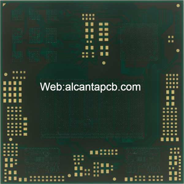
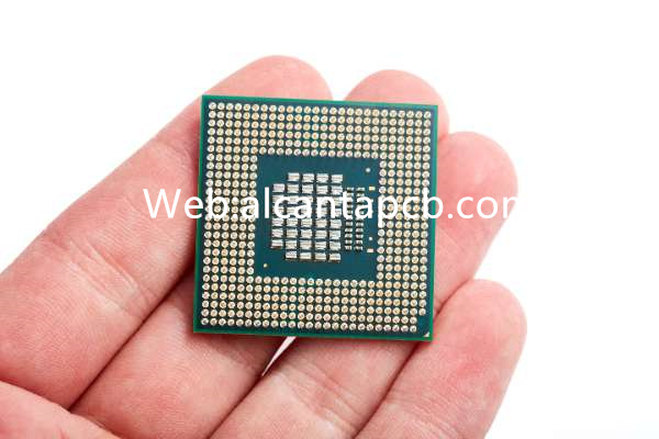
Verpackungssubstrat, oft als Verpackungssubstrat bezeichnet, ist eine der Schlüsselkomponenten in elektronischen Geräten. Es handelt sich um ein plattenartiges Material, Normalerweise besteht es aus einem isolierenden Material, das mit einer leitenden Schicht aus Kupferfolie bedeckt ist. Diese plattenartige Struktur dient als Träger und Verbinder für elektronische Bauteile, Es bietet nicht nur physische Unterstützung, sondern stellt durch seine leitenden Schichten auch Verbindungen für verschiedene elektronische Komponenten her. Diese leitende Verbindung wird durch Prozesse wie Leiterplatten erreicht (Leiterplatte) oder Chipverpackung, damit die verschiedenen Komponenten zusammenarbeiten können.
Enthüllung seiner entscheidenden Rolle in elektronischen Geräten
Verpackungssubstrate spielen in elektronischen Geräten eine entscheidende Rolle. Es bietet Unterstützung und Verbindungen, sodass elektronische Komponenten harmonisch zusammenarbeiten können, um die Funktion des Geräts zu realisieren. Als Teil der Leiterplatte, Es ist der physische Träger elektronischer Komponenten und gleichzeitig der Übertragungskanal für Signale und Energie.
Speziell, Zu den Schlüsselrollen von Verpackungssubstraten in elektronischen Geräten gehören::
Stromkreisverbindung: Die Kupferfolienschicht auf dem Verpackungssubstrat wird zur Verbindung verschiedener elektronischer Komponenten verwendet, wie zum Beispiel Chips mit integrierten Schaltkreisen, Kondensatoren und Induktivitäten. Diese Verbindung überträgt Signale und Strom zwischen verschiedenen Komponenten.
Schaltkreisisolation:Als Teil des Isoliermaterials, Das Verpackungssubstrat stellt sicher, dass sich die Schaltkreise nicht gegenseitig stören, sorgt für elektrische Isolierung und Isolierung, und sorgt für die Stabilität des Gerätes.
Mechanische Unterstützung:Das Verpackungssubstrat bietet physischen Halt für elektronische Komponenten, sie vor Schäden durch die äußere Umgebung zu schützen. Dies ist entscheidend für die Verlängerung der Lebensdauer und Zuverlässigkeit Ihrer Geräte.
Zusamenfassend, Verpackungssubstrate sind der Grundbaustein elektronischer Geräte und spielen eine Schlüsselrolle für deren Leistung, Zuverlässigkeit und Funktionalität des Gerätes. Das Verständnis ihrer Grundkonzepte und Schlüsselrollen ist entscheidend für das Verständnis der Funktionsweise moderner elektronischer Technologie.
Hauptmerkmale des Verpackungssubstrats
Materialeigenschaften
Das Material des Verpackungssubstrats ist seine Grundlage, und verschiedene Arten von Substratmaterialien beeinflussen die Leistung und Zuverlässigkeit elektronischer Geräte. Zum Beispiel, FR-4 (Flammhemmend-4) ist ein übliches glasfaserverstärktes Epoxidharzsubstrat mit guter Isolierung und mechanischer Festigkeit, und ist für allgemeine elektronische Produkte geeignet. Verbindungsplatinen mit hoher Dichte (HDI) Verwenden Sie fortschrittlichere Materialien mit höherer Leitfähigkeit und kleineren Größen, Dadurch eignen sie sich für Hochleistungsgeräte wie Smartphones und Computerchips.
Physikalische Eigenschaften
Zu den physikalischen Eigenschaften eines Verpackungssubstrats gehört seine Größe, hierarchische Struktur, und Verbindungen zwischen Schichten. Die Größe ist ein Schlüsselfaktor, da sie bestimmt, wie viele elektronische Komponenten das Substrat aufnehmen kann. Unter hierarchischer Struktur versteht man die Anordnung verschiedener Schichten auf dem Substrat, einschließlich einschichtig, Doppelschicht- und Mehrschichtstrukturen, was sich auf die Komplexität und Dichte der Schaltung auswirkt. Zwischenschichtverbindung ist die Verbindung zwischen Schichten, die zuverlässig sein müssen, um eine reibungslose Kommunikation der Schaltung zu gewährleisten.
Elektrische Eigenschaften
Die elektrischen Eigenschaften des Verpackungssubstrats haben einen wichtigen Einfluss auf die Schaltkreisleistung. Dazu gehören Eigenschaften wie Widerstand, Leitfähigkeit, und Dielektrizitätskonstante. Ein geringer Widerstand und eine hohe Leitfähigkeit können den Energieverlust bei der Signalübertragung reduzieren, Dadurch wird die Effizienz verbessert. Die Dielektrizitätskonstante beeinflusst die Signalausbreitungsgeschwindigkeit, was besonders wichtig für Hochfrequenzschaltungen ist. Die Auswahl geeigneter elektrischer Eigenschaften ist ein Schlüsselfaktor für die Gewährleistung einer stabilen Schaltungsleistung.
Diese Hauptmerkmale bestimmen gemeinsam den Anwendungsbereich und die Leistung von Verpackungssubstraten. Das Verständnis dieser Eigenschaften kann Ingenieuren dabei helfen, geeignete Substratmaterialien und Designparameter auszuwählen, um den Anforderungen einer bestimmten Anwendung gerecht zu werden, Dadurch wird die Zuverlässigkeit und Leistung elektronischer Geräte sichergestellt.
Herstellungsprozess des Verpackungssubstrats
Laminierungsprozess: Einführung in die hierarchische Strukturanordnung von Substraten
Die Herstellung von Verpackungssubstraten ist ein komplexer Prozess, Dabei ist der Laminierprozess einer der Schlüsselschritte. In dieser Phase werden verschiedene Materialschichten und Komponenten zusammengefügt, um eine mehrschichtige Struktur zu bilden, die den Anforderungen des elektronischen Geräts entspricht. Typischerweise, dazu gehört auch der Untergrund auf der unteren Schicht, die Dämmschicht in der Mitte, und die Drähte und Anschlüsse auf der obersten Schicht. Durch sorgfältige Konstruktion und Montage, Durch den Stapelprozess kann eine Schaltungskomplexität erreicht werden, die eine Vielzahl von Anwendungen unterstützt, von Leiterplatten bis hin zu Chipverpackungen.
Kupferfolienverklebung: Erläutern von Kupferfolien-Bonding-Methoden in verschiedenen Prozessen
Bei der Herstellung von Verpackungssubstraten, Die Kupferfolienverklebung ist ein entscheidender Schritt. Bei diesem Verfahren wird eine dünne Schicht Kupferfolie auf die Oberfläche des Substrats geklebt, um elektrische Verbindungen und Signalübertragung bereitzustellen. Es gibt verschiedene Methoden zum Verkleben von Kupferfolie, einschließlich stromloser Verkupferung, galvanisiertes Kupfer, und gerollte Kupferfolie. Jede Methode hat ihre Vorteile und Anwendbarkeit, und es ist wichtig, den geeigneten Prozess basierend auf den spezifischen Anwendungsanforderungen auszuwählen. Die Qualität und Stabilität der Kupferfolienbindung sind entscheidend für die Leistung des Verpackungssubstrats.
Verbindungstechnologie mit hoher Dichte: Erkundung wichtiger Schritte in der HDI-Herstellung
Bei der Herstellung von Verpackungssubstraten, hochdichte Verbindungstechnologie (HDI) ist zu einem wichtigen Bestandteil moderner elektronischer Geräte geworden. Es ermöglicht mehr Verbindungen und Kabel auf weniger Platz, zunehmende Schaltungskomplexität und Leistung. Zu den wichtigsten Schritten gehört die Bildung mikroskopischer Löcher mittels Laser oder mechanischer Methoden, um verschiedene Schaltkreisebenen zu verbinden, und sie mithilfe mikroskopisch kleiner Leiterplatten miteinander zu verbinden. Die Entwicklung der HDI-Technologie verbessert nicht nur die Leistung von Verpackungssubstraten, sondern bietet auch mehr Möglichkeiten für innovative elektronische Produkte, wie Smartphones, Tablets und drahtlose Kommunikationsgeräte.
Durch umfassendes Verständnis des Herstellungsprozesses von Verpackungssubstraten, Wir können seine Bedeutung im Bereich der Elektronik besser verstehen. Der hohe Grad an Ingenieurskunst und Präzisionsfertigung dieser kritischen Schritte gewährleistet die Zuverlässigkeit und Leistung des Verpackungssubstrats, die in der modernen Technologie unverzichtbar sind.
Anwendungsgebiete von Verpackungssubstraten
Elektronisches Produkt:Verpackungssubstrate spielen in elektronischen Geräten eine entscheidende Rolle. Erste, Es ist der Kernbestandteil der Leiterplatte (Leiterplatte), Bereitstellung von Support und Verbindungen für elektronische Komponenten. Ob es Ihr Smartphone ist, Tablet oder Laptop, Das Verpackungssubstrat ist die Grundlage für die ordnungsgemäße Funktion dieser Geräte. Zusätzlich, Verpackungssubstrate spielen auch bei der Chipverpackung eine Rolle, Schutz und Verbindung winziger integrierter Schaltkreischips. Dies bedeutet, dass jedes Mal, wenn Sie ein elektronisches Gerät verwenden, Sie interagieren mit dem Verpackungssubstrat, auch wenn es normalerweise im Inneren des Geräts versteckt ist.
Kommunikationsfeld:Verpackungssubstrate werden häufig in Kommunikationsgeräten verwendet. Besonders bei drahtlosen Kommunikationsmodulen, wie Ihr Smartphone oder WLAN-Router. Diese Geräte erfordern hochintegrierte Schaltkreise und Antennen für eine schnelle und zuverlässige Kommunikation. Die hochdichte Verbindungstechnologie von Packaging Substrate bietet diesen Geräten den nötigen Platz und die nötigen Anschlüsse, um eine stabile Signalübertragung zu gewährleisten. Zusätzlich, Der Aufstieg der 5G-Technologie hat die Nachfrage nach Verpackungssubstraten weiter erhöht, da diese höhere Frequenzbänder und eine komplexere Signalverarbeitung erfordern.
Automobilindustrie:Elektronische Systeme im Automobil werden immer komplexer, und Verpackungssubstrat spielt dabei eine Schlüsselrolle. In modernen Autos, Sie finden Verpackungssubstrate für Unterhaltungssysteme im Auto, die über Touchscreen-Bedienelemente verfügen, Audioverarbeitung, und Navigationsfunktionen. Zusätzlich, Auch die Fahrzeugsteuereinheit verlässt sich auf Packaging Substrate, um verschiedene Aspekte des Fahrzeugs zu koordinieren und zu steuern, wie Motorleistung und Sicherheitssysteme. In der Automobilindustrie, Die Zuverlässigkeit des Verpackungssubstrats ist von entscheidender Bedeutung, da es unter rauen Temperatur- und Vibrationsbedingungen betrieben werden muss.
Diese Anwendungsbereiche veranschaulichen die vielfältigen Einsatzmöglichkeiten von Verpackungssubstraten in der modernen Technologie. Ob es sich um elektronische Geräte handelt, Kommunikationsgeräte oder Automobilelektroniksysteme, Verpackungssubstrat ist eine Kernkomponente, die das ordnungsgemäße Funktionieren dieser Technologien ermöglicht, um sicherzustellen, dass sie unter verschiedenen Umgebungsbedingungen effizient arbeiten können.
Abschließend
Fassen Sie die Bedeutung und Vielfalt von Verpackungssubstraten im Elektronikbereich zusammen
Verpackungssubstrate sind aus der modernen Elektronikbranche nicht mehr wegzudenken. Es spielt eine Schlüsselrolle bei der Verbindung und Unterstützung elektronischer Komponenten, ob auf einer herkömmlichen Leiterplatte (Leiterplatte) oder in fortschrittlichen Verpackungstechnologien wie High-Density-Verbindungen (HDI). Diese Anwendungsvielfalt spiegelt sich in den unterschiedlichen Materialien wider, Größen und elektrische Eigenschaften, Bereitstellung passender Lösungen für verschiedene elektronische Geräte. Ob in Smartphones, Computer, Kfz-Steuerungssysteme, oder Kommunikationsgeräte, Verpackungssubstrat ist ein wichtiger Baustein, der die Leistung und Zuverlässigkeit dieser Geräte gewährleistet.
Mit der rasanten Entwicklung der Technologie, Packaging Substrate erfüllt nicht nur die wachsenden Leistungsanforderungen elektronischer Geräte, sondern spielt auch eine große Rolle bei der Förderung technologischer Innovationen. Die Herstellungsprozesse entwickeln sich ständig weiter, Unterstützung der Implementierung von Schaltkreisen mit hoher Dichte und Förderung der Entstehung kleinerer Schaltkreise, leichter, und leistungsfähigere elektronische Produkte. Im Bereich der modernen Kommunikation, Verpackungssubstrat ermöglicht uns eine hohe Geschwindigkeit, zuverlässige Netzwerkverbindungen, Förderung der Entwicklung der drahtlosen Kommunikation, das Internet, und das Internet der Dinge.
Zusätzlich, Zukünftige Trends bei Verpackungssubstraten legen ebenfalls Wert auf Nachhaltigkeit, mit Herstellern, die daran arbeiten, die Umweltbelastung zu reduzieren und nachhaltige Produktionsmethoden zu fördern. Dieses Umweltbewusstsein wird sicherstellen, dass Packaging Substrate weiterhin eine Schlüsselrolle nicht nur bei der technischen Leistung, sondern auch bei der Nachhaltigkeit spielt.
Um zusammenzufassen, Packaging Substrate ist ein Allrounder im Elektronikbereich. Seine Vielfalt und Unentbehrlichkeit machen unser modernes technologisches Leben komfortabler, effizient und nachhaltig. Da sich die Technologie weiterentwickelt, Packaging Substrate wird auch in Zukunft die Technologiewelt prägen. Egal in welchem Bereich Sie tätig sind, Packaging Substrate wird weiterhin solide Unterstützung für Innovation und Entwicklung leisten.