CO., LTD")
Retourner la puce (ABF) Fabricant de substrat. Flip Chip (ABF) Les fabricants de substrats se spécialisent dans la production de films de build-up avancés (ABF) substrats, essentiel pour le conditionnement de semi-conducteurs hautes performances. Ces substrats permettent des interconnexions à plus haute densité et une gestion thermique améliorée, crucial pour les applications en informatique, télécommunications, et l'industrie automobile. Les principaux fabricants exploitent une technologie de pointe et un contrôle qualité rigoureux pour fournir des produits fiables., substrats ABF de haute précision, garantir des performances et une efficacité optimales dans les appareils électroniques modernes.
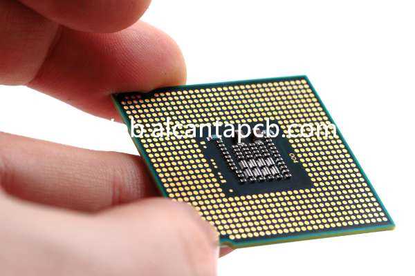
Retourner la puce (ABF) Les substrats sont avancés conditionnement matériaux utilisés pour monter et interconnecter les circuits intégrés (CI) utilisant la technologie flip chip. Ces substrats sont essentiels pour les applications de semi-conducteurs hautes performances, offrant des performances électriques améliorées, gestion thermique, et capacités de miniaturisation. Cet article approfondit les caractéristiques, considérations de conception, matériels, processus de fabrication, applications, et les avantages de Retourner la puce (ABF) Substrats.
Que sont les puces Flip (ABF) Substrats?
Retourner la puce (ABF) Les substrats sont des substrats d'emballage spécialisés qui utilisent la technologie des puces retournées., où le circuit intégré est monté face vers le bas sur le substrat, permettant des connexions électriques directes via des bosses de soudure. ABF (Film de construction Ajinomoto) est un matériau diélectrique haute performance utilisé dans ces substrats pour obtenir des capacités de lignes fines et d'espace, essentiel pour les dispositifs semi-conducteurs avancés. Ces substrats sont largement utilisés en haute densité, applications à haute vitesse telles que les processeurs, dispositifs de mémoire, et systèmes de communication avancés.
Considérations de conception pour la puce Flip (ABF) Substrats
Conception d'une puce Flip (ABF) Les substrats impliquent plusieurs considérations critiques:
Choisir les bons matériaux avec des propriétés diélectriques appropriées, conductivité thermique, et la résistance mécanique est cruciale pour des performances optimales.
Une gestion thermique efficace est essentielle pour éviter la surchauffe et garantir un fonctionnement fiable. Cela inclut l'incorporation de vias thermiques, dissipateurs de chaleur, et autres mécanismes de refroidissement.
Le maintien de l'intégrité du signal à hautes fréquences nécessite un contrôle minutieux de l'impédance de trace, minimiser la diaphonie, et mettre en œuvre des techniques efficaces de mise à la terre et de blindage.
Le substrat doit avoir une résistance mécanique et une stabilité suffisantes pour résister aux processus de fabrication et aux conditions opérationnelles., y compris les cycles thermiques et les contraintes mécaniques.
La finition de surface doit être lisse et sans défaut pour garantir une bonne adhérence et un bon alignement des composants et minimiser la perte de signal et la réflexion..
Matériaux utilisés dans la puce Flip (ABF) Substrats
Plusieurs matériaux sont couramment utilisés dans la fabrication des Flip Chip (ABF) Substrats:
L'ABF est un matériau diélectrique haute performance qui offre d'excellentes propriétés électriques, capacités de lignes fines, et résistance mécanique.
Une feuille de cuivre de haute qualité est utilisée pour les traces conductrices et les vias, offrant une excellente conductivité électrique et une excellente fiabilité.
Des résines époxy haute performance sont utilisées comme matériaux adhésifs pour lier les couches du substrat entre elles., offrant résistance mécanique et stabilité.
Ceux-ci sont appliqués sur les plages de contact pour améliorer la soudabilité et protéger contre l'oxydation..
Dans certains cas, les céramiques comme l'alumine (Al2O3) ou nitrure d'aluminium (AIN) peuvent être utilisés pour leur excellente conductivité thermique et leurs propriétés mécaniques.
Processus de fabrication de puces retournées (ABF) Substrats
Le processus de fabrication du Flip Chip (ABF) Les substrats impliquent plusieurs étapes précises:
Les matières premières, dont ABF, feuille de cuivre, et résines époxy, sont préparés et transformés en feuilles ou en rouleaux.
Plusieurs couches du matériau de substrat sont stratifiées ensemble pour former une structure de construction. Ce processus consiste à appliquer de la chaleur et de la pression pour lier les couches.
Les modèles de circuits sont créés à l'aide de processus photolithographiques. Un film photosensible (photorésist) est appliqué sur le support, exposé aux ultraviolets (UV) lumière à travers un masque, et développé pour révéler les modèles de circuits souhaités. Le substrat est ensuite gravé pour éliminer les matériaux indésirables.
Des vias sont percés dans le substrat pour créer des connexions électriques verticales entre les différentes couches. Ces trous sont ensuite plaqués de cuivre pour établir des chemins conducteurs.
Un lisse, une finition de surface sans défaut est appliquée sur les plages de contact pour garantir une adhérence et un alignement corrects des composants, ainsi que pour minimiser la perte de signal et la réflexion.
Les substrats finis sont soumis à des tests et à une inspection rigoureux pour garantir qu'ils répondent aux spécifications requises en matière de performances électriques., intégrité du signal, et la fiabilité.
Applications de la puce Flip (ABF) Substrats
Retourner la puce (ABF) Les substrats sont utilisés dans une large gamme d'applications hautes performances:
Ces substrats sont utilisés dans les processeurs et microcontrôleurs hautes performances, fournissant les propriétés électriques et thermiques nécessaires pour un fonctionnement fiable.
Retourner la puce (ABF) Les substrats sont utilisés dans les dispositifs de mémoire, y compris DRAM et mémoire flash, où les interconnexions haute densité et l’intégrité du signal sont cruciales.
Ces substrats prennent en charge les systèmes de communication avancés, y compris les stations de base 5G et l'infrastructure réseau, où le fonctionnement à grande vitesse et l’intégrité du signal sont essentiels.
Retourner la puce (ABF) Les substrats sont utilisés dans l'électronique grand public, comme les smartphones, comprimés, et appareils portables, où la miniaturisation et la performance sont essentielles.
Les substrats sont utilisés dans l'électronique automobile, y compris des systèmes avancés d’aide à la conduite (ADAS) et systèmes d'infodivertissement, exigeant des performances et une fiabilité robustes.
Avantages de la puce Flip (ABF) Substrats
Retourner la puce (ABF) Les substrats offrent plusieurs avantages:
L'utilisation d'ABF permet d'obtenir des lignes fines et des caractéristiques spatiales, permettant les interconnexions haute densité nécessaires aux dispositifs semi-conducteurs avancés.
Ces substrats offrent d'excellentes performances électriques, y compris une faible perte de signal et une intégrité élevée du signal, crucial pour les applications à grande vitesse.
Les matériaux à haute conductivité thermique assurent une dissipation thermique efficace, éviter la surchauffe et assurer un fonctionnement fiable.
Les substrats offrent un support mécanique robuste, assurer la fiabilité et la durabilité des composants emballés dans diverses conditions environnementales.
La capacité de créer des fonctionnalités fines et des interconnexions haute densité prend en charge la miniaturisation des boîtiers semi-conducteurs, ce qui les rend adaptés aux appareils électroniques compacts.
FAQ
Quels sont les principaux avantages de l'utilisation de Flip Chip (ABF) Substrats?
Les principaux avantages incluent des interconnexions haute densité, performances électriques supérieures, gestion thermique efficace, stabilité mécanique, et prise en charge de la miniaturisation. Ces substrats constituent la base de la fabrication de dispositifs semi-conducteurs hautes performances.
Quels matériaux sont couramment utilisés dans Flip Chip (ABF) Substrats?
Les matériaux courants incluent l'ABF (Film de construction Ajinomoto), feuille de cuivre, résines époxy hautes performances, finitions nickel/or, et, dans certains cas, céramiques hautes performances telles que l'alumine ou le nitrure d'aluminium.
Comment se déroule la conception d’un Flip Chip (ABF) Le substrat garantit l'intégrité du signal?
La conception garantit l'intégrité du signal en fournissant de faibles valeurs de constante diélectrique et de tangente de perte, contrôle de l'impédance de trace, minimiser la diaphonie, et mettre en œuvre des techniques efficaces de mise à la terre et de blindage. Des outils de simulation sont utilisés pour optimiser ces aspects pour les performances haute fréquence.
Quelles sont les applications courantes de Flip Chip (ABF) Substrats?
Les applications courantes incluent les processeurs et les microcontrôleurs, dispositifs de mémoire, systèmes de communication avancés, électronique grand public, et électronique automobile. Ces substrats sont utilisés dans les systèmes nécessitant des interconnexions haute densité, performances électriques supérieures, et une gestion thermique efficace.