CO., LTD")
Fabricant de substrats de packages RF.Un RF Packages substrats Le fabricant est spécialisé dans la production de substrats hautes performances pour les applications RF, permettant une transmission efficace du signal et une gestion thermique supérieure. Avec des techniques de fabrication avancées, ils fournissent des solutions personnalisées pour répondre aux exigences strictes du secteur des télécommunications, aérospatial, et industries de défense. Leur expertise garantit la fiabilité et des performances améliorées dans les systèmes RF critiques.
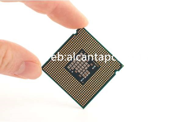
RF (Radiofréquence) Emballer Substrats sont des composants essentiels dans la fabrication d’appareils électroniques fonctionnant aux radiofréquences, y compris les systèmes de communication sans fil, radar, et communications par satellite. Ces substrats sont conçus pour fournir une excellente intégrité du signal, gestion thermique, et stabilité mécanique, ce qui les rend idéaux pour les applications haute fréquence. Cet article explore les fonctionnalités, considérations de conception, matériels, processus de fabrication, applications, et avantages des substrats RF Package.
Que sont les substrats de package RF?
Les substrats RF Package sont des matériaux spécialisés utilisés dans l'emballage de composants électroniques RF.. Ils servent de base au montage et à l'interconnexion de divers appareils électroniques, y compris les circuits intégrés (CI), résistances, condensateurs, et inducteurs. Ces substrats sont conçus pour minimiser la perte et la distorsion du signal, assurer une gestion thermique efficace, et fournir un support mécanique. Ils sont essentiels au maintien des performances et de la fiabilité des systèmes RF.
Considérations de conception pour les substrats de boîtiers RF
La conception de substrats de packages RF implique plusieurs considérations critiques:
Choisir les bons matériaux avec des propriétés diélectriques appropriées, conductivité thermique, et la résistance mécanique est cruciale pour des performances optimales.
Une gestion thermique efficace est essentielle pour éviter la surchauffe et garantir un fonctionnement fiable. Cela inclut l'incorporation de vias thermiques, dissipateurs de chaleur, et autres mécanismes de refroidissement.
Le maintien de l'intégrité du signal à hautes fréquences nécessite un contrôle minutieux de l'impédance de trace, minimiser la diaphonie, et mettre en œuvre des techniques efficaces de mise à la terre et de blindage.
Le substrat doit avoir une résistance mécanique et une stabilité suffisantes pour résister aux processus de fabrication et aux conditions opérationnelles., y compris les cycles thermiques et les contraintes mécaniques.
La finition de surface doit être lisse et sans défaut pour garantir une bonne adhérence et un bon alignement des composants et minimiser la perte de signal et la réflexion..
Matériaux utilisés dans les substrats de boîtiers RF
Plusieurs matériaux sont couramment utilisés dans la fabrication de substrats de boîtiers RF.:
Des matériaux tels que l'alumine (Al2O3), nitrure d'aluminium (AIN), et oxyde de béryllium (BeO) offrent d'excellentes propriétés diélectriques et une conductivité thermique élevée.
Stratifiés haute fréquence, comme le PTFE (polytétrafluoroéthylène) et composites PTFE chargés de céramique, fournissent de faibles valeurs de constante diélectrique et de tangente de perte, garantissant une perte de signal minimale.
Le cuivre et d'autres alliages métalliques sont utilisés pour les traces et vias conducteurs en raison de leur excellente conductivité électrique et de leur fiabilité..
Des résines époxy haute performance sont utilisées comme matériaux adhésifs pour lier les couches du substrat entre elles., offrant résistance mécanique et stabilité.
Ceux-ci sont appliqués sur les plages de contact pour améliorer la soudabilité et protéger contre l'oxydation..
Processus de fabrication des substrats de boîtiers RF
Le processus de fabrication des substrats RF Package implique plusieurs étapes précises:
Les matières premières, y compris les céramiques hautes performances, stratifiés organiques, et alliages métalliques, sont préparés et transformés en feuilles ou en films.
Plusieurs couches du matériau de substrat sont stratifiées ensemble pour former une structure de construction. Ce processus consiste à appliquer de la chaleur et de la pression pour lier les couches.
Les modèles de circuits sont créés à l'aide de processus photolithographiques. Un film photosensible (photorésist) est appliqué sur le support, exposé aux ultraviolets (UV) lumière à travers un masque, et développé pour révéler les modèles de circuits souhaités. Le substrat est ensuite gravé pour éliminer les matériaux indésirables.
Des vias sont percés dans le substrat pour créer des connexions électriques verticales entre les différentes couches. Ces trous sont ensuite plaqués de cuivre pour établir des chemins conducteurs.
Un lisse, une finition de surface sans défaut est appliquée sur les plages de contact pour garantir une adhérence et un alignement corrects des composants, ainsi que pour minimiser la perte de signal et la réflexion.
Les substrats finis sont soumis à des tests et à une inspection rigoureux pour garantir qu'ils répondent aux spécifications requises en matière de performances électriques., intégrité du signal, et la fiabilité.
Applications des substrats de package RF
Les substrats RF Package sont utilisés dans une large gamme d’applications haute fréquence:
Ces substrats prennent en charge le packaging de composants RF dans les téléphones mobiles, stations de base, Routeurs Wi-Fi, et autres appareils de communication sans fil.
Les substrats RF Package sont utilisés dans les systèmes radar utilisés dans l'automobile, aviation, et applications de défense, où le fonctionnement et la fiabilité à haute fréquence sont essentiels.
Ces substrats sont utilisés dans les systèmes de communication par satellite, y compris les transpondeurs satellite et l'équipement de la station au sol, garantissant une intégrité et des performances élevées du signal.
Les substrats RF Package sont utilisés dans les dispositifs et équipements médicaux, tels que les appareils IRM et les systèmes de surveillance des patients sans fil, où un fonctionnement haute fréquence fiable est essentiel.
Les substrats sont utilisés dans les applications aérospatiales et de défense, y compris les systèmes de communication, guerre électronique, et systèmes de guidage, là où des performances robustes et une fiabilité sont requises.
Avantages des substrats de package RF
Les substrats RF Package offrent plusieurs avantages:
Les faibles valeurs de constante diélectrique et de tangente de perte garantissent une perte et une distorsion minimales du signal, maintenir une fidélité et des performances élevées du signal.
Les matériaux à haute conductivité thermique assurent une dissipation thermique efficace, éviter la surchauffe et assurer un fonctionnement fiable.
Les substrats offrent un support mécanique robuste, assurer la fiabilité et la durabilité des composants emballés dans diverses conditions environnementales.
Les substrats RF Package sont compatibles avec une large gamme de composants RF et peuvent s'adapter à diverses techniques de montage et d'interconnexion..
Ces substrats peuvent être personnalisés pour répondre à des exigences de conception spécifiques, y compris l'incorporation de matériaux spécifiques, configurations de couches, et finitions de surface.
FAQ
Quels sont les principaux avantages de l'utilisation des substrats RF Package?
Les principaux avantages incluent une intégrité élevée du signal, gestion thermique efficace, stabilité mécanique, compatibilité avec les composants RF, et personnalisation. Ces substrats constituent la base de la fabrication de dispositifs électroniques RF hautes performances avec une intégrité de signal fiable et une gestion thermique efficace..
Quels matériaux sont couramment utilisés dans les substrats de packages RF?
Les matériaux courants incluent la céramique haute performance (comme l'alumine, nitrure d'aluminium, et oxyde de béryllium), stratifiés organiques (tels que le PTFE et les composites de PTFE chargés en céramique), alliages métalliques (comme le cuivre), résines époxy, et finitions nickel/or. Ces matériaux offrent d'excellentes propriétés diélectriques, conductivité thermique, et résistance mécanique.
Comment la conception d'un substrat de boîtier RF garantit-elle l'intégrité du signal?
La conception garantit l'intégrité du signal en fournissant de faibles valeurs de constante diélectrique et de tangente de perte, contrôle de l'impédance de trace, minimiser la diaphonie, et mettre en œuvre des techniques efficaces de mise à la terre et de blindage. Des outils de simulation sont utilisés pour optimiser ces aspects pour les performances haute fréquence.
Quelles sont les applications courantes des substrats RF Package?
Les applications courantes incluent les systèmes de communication sans fil, systèmes radar, communications par satellite, dispositifs médicaux, et aérospatiale et défense. Ces substrats sont utilisés dans les systèmes nécessitant une intégrité élevée du signal, gestion thermique efficace, et des performances et une fiabilité robustes.