CO.,LTD")
Hersteller von Flip-Chip-Ball-Grid-Array-Substraten. Als führender Anbieter Flip-Chip Hersteller von Ball Grid Array-Substraten, Wir sind auf die Herstellung von Hochleistungssubstraten für fortschrittliche elektronische Anwendungen spezialisiert. Unsere hochmodernen Fertigungsprozesse gewährleisten höchste Qualität und Zuverlässigkeit, Erfüllung der Anforderungen von Branchen wie der Telekommunikation, Rechnen, und Automobil. Durch den Einsatz modernster Technologie und innovativem Design, Wir bieten Lösungen, die die Geräteleistung verbessern, unterstützen die Miniaturisierung, und sorgen für eine robuste thermische und Signalintegrität.
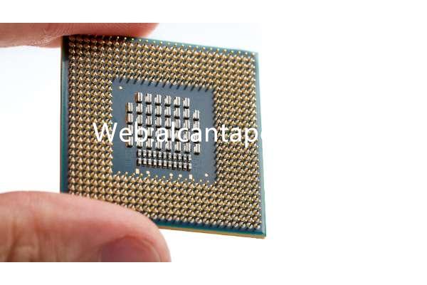
Das Flip-Chip-Ball-Grid-Array (FC-BGA) Substrat ist ein entscheidender Bestandteil moderner elektronischer Verpackungen, bietet eine robuste Lösung für Hochleistungs- und High-Density-Anwendungen. FC-BGA-Substrate sind für die Unterstützung fortschrittlicher Halbleiterchips konzipiert, Bereitstellung elektrischer Anschlüsse, mechanische Unterstützung, und Wärmeableitung. Diese Substrate spielen eine entscheidende Rolle bei der Verbesserung der Leistung und Zuverlässigkeit integrierter Schaltkreise (ICs) in verschiedenen Anwendungen, von Unterhaltungselektronik bis hin zu Automobilsystemen. In diesem Artikel, Wir werden uns mit den Feinheiten von FC-BGA-Substraten befassen, ihre Struktur erforschen, Materialien, Herstellungsprozesse, Anwendungsbereiche, und Vorteile.
Was ist ein FC-BGA-Substrat??
Ein FC-BGA-Substrat ist eine Art Verpackungstechnologie, mit der Halbleiterchips mit Löthöckern direkt auf einem Substrat montiert werden. Im Gegensatz zu herkömmlicher Drahtbindung, Bei der Flip-Chip-Technologie wird der Chip auf den Kopf gestellt, So dass der aktive Bereich dem Substrat zugewandt ist. Diese Methode bietet mehrere Vorteile, einschließlich Verbindungen mit höherer Dichte, Verbesserte elektrische Leistung, und besseres Wärmemanagement.
Das FC-BGA-Substrat besteht aus mehreren Schichten, einschließlich einer Kernschicht, Aufbauschichten, und Lötmaskenschichten. Die Kernschicht besteht typischerweise aus Materialien wie Bismaleimidtriazin (Bt) Harz oder Epoxidharz, die eine hervorragende thermische Stabilität und mechanische Festigkeit bieten. Aufbauschichten, Hergestellt aus dielektrischen Materialien und Kupfer, werden hinzugefügt, um die komplizierte Verkabelung zu erstellen, die für hochdichte Verbindungen erforderlich ist. Lötstoppschichten schützen die Schaltkreise und verhindern die Bildung von Lötbrücken während der Montage.
Die Verbindungen zwischen dem Chip und dem Substrat werden mithilfe von Löthöckern hergestellt, Dabei handelt es sich um kleine Kügelchen aus Lötmaterial, die auf den I/O-Pads des Chips platziert werden. Während der Montage, Der Chip wird umgedreht und am Substrat ausgerichtet, und die Löthöcker werden aufgeschmolzen, um eine robuste mechanische und elektrische Verbindung herzustellen. Dieser Prozess ermöglicht im Vergleich zum herkömmlichen Drahtbonden eine höhere Anzahl von Verbindungen pro Flächeneinheit.
Struktur von FC-BGA-Substraten
Die Struktur von FC-BGA-Substraten ist komplex und hochentwickelt, um den Anforderungen moderner Halbleiterverpackungen gerecht zu werden. Die Substrate bestehen typischerweise aus mehreren Schlüsselkomponenten:
Die Kernschicht bildet das mechanische Rückgrat des Substrats. Materialien wie BT-Harz oder Epoxidharz werden aufgrund ihrer hervorragenden thermischen und mechanischen Eigenschaften häufig verwendet. Die Kernschicht ist typischerweise starr, Bietet Stabilität und Halt für die gesamte Substratstruktur.
Auf beiden Seiten der Kernschicht werden mehrere Aufbauschichten hinzugefügt, um die notwendige Führung für elektrische Signale zu schaffen. Diese Schichten bestehen aus dielektrischen Materialien, wie harzbeschichtetes Kupfer (RCC) oder Epoxidharz, und sind mit Kupferspuren durchsetzt. Die Aufbauschichten ermöglichen die für fortschrittliche ICs erforderliche Verdrahtung mit hoher Dichte, Dies ermöglicht kompliziertes Routing und mehrere Verbindungsebenen.
Über den Aufbauschichten werden Lötstoppschichten aufgebracht, um die Schaltkreise zu schützen und Lötbrücken zu verhindern. Diese Schichten bestehen aus isolierenden Materialien und sind entscheidend für die Aufrechterhaltung der Integrität der elektrischen Verbindungen während der Montage und des Betriebs.
Löthöcker sind kleine Kügelchen aus Lötmaterial, die auf den I/O-Pads des Chips platziert werden. Diese Bumps stellen die elektrische und mechanische Verbindung zwischen Chip und Substrat her. Die Löthöcker bestehen typischerweise aus bleifreien Lötmaterialien, wie Zinn-Silber-Kupfer (SACK) Legierungen, Umweltvorschriften einzuhalten.
Die Gesamtstruktur eines FC-BGA-Substrats ist darauf ausgelegt, die elektrische Leistung zu optimieren, Wärmemanagement, und mechanische Stabilität. Die Kombination von Kernschichten, Aufbauschichten, Lötmaskenschichten, und Löthöcker gewährleisten einen zuverlässigen Betrieb in anspruchsvollen Anwendungen.
In FC-BGA-Substraten verwendete Materialien
Die in FC-BGA-Substraten verwendeten Materialien werden sorgfältig ausgewählt, um den strengen Anforderungen leistungsstarker Halbleiterverpackungen gerecht zu werden. Zu den wichtigsten Materialien gehören::
Die Kernschicht besteht typischerweise aus BT-Harz oder Epoxidharz. BT-Harz wird wegen seiner hervorragenden thermischen Stabilität bevorzugt, niedrige Dielektrizitätskonstante, und gute mechanische Festigkeit. Epoxidmaterialien werden auch wegen ihrer Kosteneffizienz und angemessenen Leistung in vielen Anwendungen verwendet.
Die Aufbauschichten verwenden dielektrische Materialien wie RCC oder Epoxidharz, um die Kupferleiterbahnen zu isolieren und für strukturelle Integrität zu sorgen. RCC-Materialien sind für ihre geringe Wärmeausdehnung und hohe Zuverlässigkeit bekannt, Dadurch eignen sie sich für Verbindungen mit hoher Dichte.
Für die Leiterbahnen in den Aufbauschichten wird häufig Kupfer verwendet. Es bietet eine hervorragende elektrische Leitfähigkeit, Wärmeleitfähigkeit, und Zuverlässigkeit. Die Kupferschichten werden typischerweise durch Galvanisierungsverfahren gebildet, Dies ermöglicht eine präzise Kontrolle der Leiterbahnabmessungen und -dicke.
Die Lötmaskenschichten bestehen aus isolierenden Materialien, die die darunter liegende Schaltung schützen und die Bildung von Lötbrücken verhindern. Diese Materialien basieren typischerweise auf Epoxidharz und werden mithilfe von Siebdruck- oder Fotoabbildungstechniken aufgetragen.
Löthöcker bestehen aus bleifreien Lötmaterialien, wie SAC-Legierungen. Diese Materialien bieten gute mechanische Eigenschaften, ausgezeichnete thermische Ermüdungsbeständigkeit, und Einhaltung von Umweltvorschriften.
Die sorgfältige Auswahl und Kombination dieser Materialien ist entscheidend für die Erzielung der gewünschten elektrischen Eigenschaften, Thermal-, und mechanische Leistung von FC-BGA-Substraten. Jedes Material trägt zur Gesamtzuverlässigkeit und Leistung des Substrats bei, um sicherzustellen, dass es den Anforderungen moderner Halbleiterverpackungen gerecht wird.
TDer Herstellungsprozess von FC-BGA-Substraten
Der Herstellungsprozess von FC-BGA-Substraten umfasst mehrere komplizierte Schritte, Jeder trägt zur Gesamtqualität und Leistung des Endprodukts bei. Der Prozess umfasst:
Im ersten Schritt werden die Kernmaterialien vorbereitet, dielektrische Materialien, und Kupferfolien. Die Kernmaterialien werden typischerweise mit Kupferfolien laminiert, um das Ausgangssubstrat zu bilden.
Für mehrschichtige Untergründe, Mehrere Schichten aus Dielektrikum und Kupfer werden gestapelt und durch Laminierungsverfahren miteinander verbunden. Dieser Schritt erfordert eine präzise Ausrichtung und Kontrolle, um eine ordnungsgemäße Ausrichtung und Verbindung jeder Schicht sicherzustellen.
Nach dem Schichtenstapeln, Löcher werden in das Substrat gebohrt, um Durchkontaktierungen und Durchgangslöcher zu erzeugen. Fortgeschrittene Bohrtechniken, wie Laserbohren, einsetzbar für Microvias und hochpräzise Anforderungen. Anschließend werden die Bohrlöcher gereinigt und für die Beschichtung vorbereitet.
Die Bohrlöcher werden mit Kupfer beschichtet, um elektrische Verbindungen zwischen den Schichten herzustellen. Dabei wird durch galvanische Verfahren eine dünne Kupferschicht auf die Lochwände aufgetragen. Der Beschichtungsprozess muss sorgfältig kontrolliert werden, um eine gleichmäßige Abdeckung und Haftung sicherzustellen.
Die gewünschten Schaltkreismuster werden mit einem fotolithografischen Verfahren auf die Kupferschichten übertragen. Dabei wird ein lichtempfindlicher Film aufgebracht (Fotolack) auf die Kupferoberfläche und setzt sie ultraviolettem Licht aus (UV) Licht durch eine Fotomaske. Die belichteten Bereiche des Fotolacks werden entwickelt, Das Schaltungsmuster bleibt zurück. Anschließend wird die Platine geätzt, um das unerwünschte Kupfer zu entfernen, Es bleiben nur die Leiterbahnen übrig.
Auf die Platine wird eine Lötmaske aufgetragen, um die Schaltkreise zu schützen und Lötbrücken zu verhindern. Die Lötstoppmaske wird typischerweise mit Siebdruck- oder Fotoabbildungstechniken aufgetragen und anschließend ausgehärtet, um sie auszuhärten.
Auf die freiliegenden Kupferbereiche wird eine Oberflächenveredelung aufgetragen, um die Lötbarkeit zu verbessern und vor Oxidation zu schützen. Zu den gängigen Oberflächenveredelungen gehört Chemisch-Nickel-Immersionsgold (ZUSTIMMEN), Heißluft-Lotnivellierung (Bluten), und Immersionssilber.
Auf den I/O-Pads des Chips werden Löthöcker platziert, Anschließend wird der Chip umgedreht und am Substrat ausgerichtet. Die Löthöcker werden aufgeschmolzen, um eine robuste mechanische und elektrische Verbindung zwischen dem Chip und dem Substrat herzustellen.
Der letzte Schritt umfasst strenge Tests und Inspektionen, um sicherzustellen, dass das Substrat alle Leistungs- und Zuverlässigkeitsanforderungen erfüllt. Elektrische Prüfung, Sichtprüfung, und automatisierte optische Inspektion (AOI) dienen der Feststellung etwaiger Mängel oder Unregelmäßigkeiten. Alle während der Tests festgestellten Probleme werden behoben, bevor die Substrate für den Versand freigegeben werden.
Der Herstellungsprozess von FC-BGA-Substraten erfordert eine präzise Kontrolle und Fachwissen, um hohe Qualität und Zuverlässigkeit sicherzustellen. Jeder Schritt ist entscheidend für das Erreichen der gewünschten Leistung und Zuverlässigkeit des Endprodukts.
Anwendungsbereiche von FC-BGA-Substraten
FC-BGA-Substrate werden aufgrund ihrer hohen Leistung und Zuverlässigkeit in einer Vielzahl von Anwendungen in verschiedenen Branchen eingesetzt. Zu den wichtigsten Anwendungsbereichen gehören:
FC-BGA-Substrate werden häufig in der Unterhaltungselektronik verwendet, wie Smartphones, Tabletten, und Gaming -Konsolen. Diese Geräte erfordern Hochleistungs-ICs mit fortschrittlichen Verpackungslösungen, um die gewünschte Leistung und den gewünschten Formfaktor zu erreichen. FC-BGA-Substrate sorgen für die notwendigen Verbindungen, Wärmemanagement, und mechanische Unterstützung für diese Hochleistungschips.
Die Automobilindustrie ist für verschiedene Anwendungen auf fortschrittliche Elektronik angewiesen, einschließlich Motorsteuergeräten (ABDECKUNG), fortschrittliche Fahrerassistenzsysteme (Adas), und Infotainmentsysteme. FC-BGA-Substrate bieten eine hohe Zuverlässigkeit, Wärmemanagement, und mechanische Stabilität, die für Automobilanwendungen erforderlich ist, Gewährleistung des sicheren und effizienten Betriebs elektronischer Systeme in Fahrzeugen.
In der Telekommunikation, FC-BGA-Substrate werden in Basisstationen verwendet, Netzwerkinfrastruktur, und Kommunikationsgeräte. Die hochdichten Verbindungen und die überlegene elektrische Leistung von FC-BGA-Substraten machen sie ideal für die Verarbeitung der in modernen Kommunikationssystemen erforderlichen Hochfrequenzsignale und Datenraten.
Medizinische Geräte, wie beispielsweise bildgebende Systeme, Diagnosegeräte, und Patientenüberwachungsgeräte, erfordern leistungsstarke und zuverlässige ICs. FC-BGA-Substrate sorgen für die nötige elektrische Leistung, Wärmemanagement, und Zuverlässigkeit für diese kritischen Anwendungen, Gewährleistung eines genauen und konsistenten Betriebs medizinischer Geräte.
In der Industrieelektronik, FC-BGA-Substrate werden in Automatisierungssystemen verwendet, Energieverwaltung, und Steuerungssysteme. Diese Anwendungen erfordern robuste und zuverlässige Verpackungslösungen, um rauen Umgebungsbedingungen standzuhalten und einen kontinuierlichen Betrieb zu gewährleisten. FC-BGA-Substrate bieten die nötige Leistung und Haltbarkeit für industrielle Anwendungen.
Luft- und Raumfahrt- und Verteidigungsanwendungen erfordern hochzuverlässige und leistungsstarke elektronische Systeme. FC-BGA-Substrate werden in Radarsystemen verwendet, Kommunikationsausrüstung, und Avionik, Bereitstellung der notwendigen elektrischen Leistung, Wärmemanagement, und mechanische Stabilität für geschäftskritische Anwendungen.
Vorteile von FC-BGA-Substraten
FC-BGA-Substrate bieten mehrere Vorteile, die sie zu einer bevorzugten Wahl für Hochleistungs- und Hochzuverlässigkeitsanwendungen machen. Zu diesen Vorteilen gehören:
FC-BGA-Substrate ermöglichen eine hohe Anzahl von Verbindungen pro Flächeneinheit, Dies ermöglicht komplexere und leistungsfähigere IC-Designs. Diese hohe Dichte wird durch die Verwendung von Löthöckern und fortschrittlichen Mehrschichtstrukturen erreicht, Bietet überragende elektrische Leistung und Signalintegrität.
Die in FC-BGA-Substraten verwendete Flip-Chip-Technologie bietet im Vergleich zum herkömmlichen Drahtbonden kürzere und direktere Signalwege. Dies führt zu einem geringeren Signalverlust, reduzierte parasitäre Induktivität und Kapazität, und verbesserte Signalintegrität, Dadurch sind FC-BGA-Substrate ideal für Hochfrequenz- und Hochgeschwindigkeitsanwendungen.
FC-BGA-Substrate bieten ein effizientes Wärmemanagement durch die Verwendung von Materialien mit hoher Wärmeleitfähigkeit und optimierten Strukturen. Die Flip-Chip-Konfiguration ermöglicht außerdem eine direkte Wärmeableitung vom Chip zum Substrat, Reduzierung des Wärmewiderstands und Verbesserung der Wärmeableitung. Dies ist von entscheidender Bedeutung für Hochleistungsanwendungen, bei denen ein effektives Wärmemanagement für einen zuverlässigen Betrieb unerlässlich ist.
Die robuste Struktur von FC-BGA-Substraten, einschließlich der Verwendung von BT-Harz oder Epoxidkernmaterialien, bietet hervorragende mechanische Stabilität und Zuverlässigkeit. Dadurch wird sichergestellt, dass die Untergründe mechanischen Belastungen standhalten, Thermalradfahren, und rauen Umgebungsbedingungen, ohne die Leistung zu beeinträchtigen.
FC-BGA-Substrate bieten Skalierbarkeit sowohl hinsichtlich der Leistung als auch der Herstellung. Die Technologie ermöglicht die Integration mehrerer Chips und Funktionen auf einem einzigen Substrat, Ermöglicht die Entwicklung fortschrittlicher System-in-Package (Schluck) Lösungen. Zusätzlich, Die Herstellungsprozesse für FC-BGA-Substrate sind mit der Massenproduktion kompatibel, Dadurch eignen sie sich sowohl für kostengünstige Unterhaltungselektronik als auch für hochwertige Industrieanwendungen.
FC-BGA-Substrate sind vielseitig und können in einer Vielzahl von Anwendungen eingesetzt werden, von der Unterhaltungselektronik bis zur Automobilindustrie, Telekommunikation, Medizinprodukte, Industrieelektronik, und Luft- und Raumfahrt und Verteidigung. Die Kombination aus hoher Leistung, Zuverlässigkeit, und Skalierbarkeit machen FC-BGA-Substrate zu einer idealen Wahl für verschiedene Branchen und Anwendungen.
FAQ
Was unterscheidet FC-BGA-Substrate von herkömmlichen BGA-Substraten??
FC-BGA-Substrate unterscheiden sich von herkömmlichen BGA-Substraten hauptsächlich durch die Verwendung der Flip-Chip-Technologie. In FC-BGA-Substraten, Der Chip wird umgedreht und über Löthöcker mit dem Substrat verbunden, Dies führt zu einer höheren Verbindungsdichte, Verbesserte elektrische Leistung, und besseres Wärmemanagement. Herkömmliche BGA-Substrate verwenden Drahtbonden, die bei Hochfrequenz- und Hochleistungsanwendungen möglicherweise nicht das gleiche Leistungsniveau bieten.
Können FC-BGA-Substrate in Hochleistungsanwendungen verwendet werden??
Ja, FC-BGA-Substrate eignen sich gut für Hochleistungsanwendungen. Die Flip-Chip-Konfiguration ermöglicht eine direkte Wärmeableitung vom Chip zum Substrat, Reduzierung des Wärmewiderstands und Verbesserung des Wärmemanagements. Dadurch sind FC-BGA-Substrate ideal für Anwendungen wie Leistungsverstärker, Automobilelektronik, und Industrieanlagen, bei denen eine effektive Wärmeableitung für einen zuverlässigen Betrieb entscheidend ist.
Sind FC-BGA-Substrate für den Einsatz in rauen Umgebungen geeignet??
FC-BGA-Substrate eignen sich hervorragend für den Einsatz in rauen Umgebungen. Die robuste Struktur, einschließlich der Verwendung von Materialien mit hervorragenden thermischen und mechanischen Eigenschaften, sorgt für zuverlässige Leistung unter wechselnden Umgebungsbedingungen, wie zum Beispiel hohe Temperaturen, Luftfeuchtigkeit, und mechanische Beanspruchung. Dies macht FC-BGA-Substrate zu einer ausgezeichneten Wahl für die Automobilindustrie, Luft- und Raumfahrt, und Verteidigungsanwendungen, bei denen Zuverlässigkeit unter extremen Bedingungen von entscheidender Bedeutung ist.
Wie gewährleistet der Herstellungsprozess von FC-BGA-Substraten eine hohe Qualität und Zuverlässigkeit??
Der Herstellungsprozess von FC-BGA-Substraten umfasst mehrere komplizierte Schritte, inklusive Materialvorbereitung, Schichtstapelung, Bohren, Überzug, Bildgebung, Radierung, Auftragen einer Lötstoppmaske, Oberflächenveredelung, Platzierung der Löthöcker, und strenge Tests und Inspektionen. Jeder Schritt wird sorgfältig kontrolliert und überwacht, um eine hohe Qualität und Zuverlässigkeit zu gewährleisten. Fortgeschrittene Techniken wie Laserbohren, Galvanisieren, und automatisierte optische Inspektion (AOI) werden verwendet, um präzise und konsistente Ergebnisse zu erzielen. Dieser sorgfältige Prozess stellt sicher, dass FC-BGA-Substrate die strengen Leistungs- und Zuverlässigkeitsanforderungen von Hochleistungs-Halbleitergehäusen erfüllen.