КОМПАНИЯ С ОГРАНИЧЕННОЙ ОТВЕТСТВЕННОСТЬЮ")
Производитель подложек с решетчатыми шариками с флип-чипом. В качестве ведущего производителя Флип-чип Производитель подложек с шариковой решеткой, мы специализируемся на производстве высокопроизводительных подложек для передовых электронных приложений.. Наши современные производственные процессы обеспечивают превосходное качество и надежность., удовлетворение потребностей таких отраслей, как телекоммуникации, вычисления, и автомобилестроение. Используя передовые технологии и инновационный дизайн., мы предоставляем решения, повышающие производительность устройств, поддержка миниатюризации, и обеспечить надежную тепловую целостность и целостность сигнала.
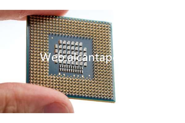
Сетка из шариков Flip Chip (FC-BGA) субстрат является важнейшим компонентом современной электронной упаковки., предлагая надежное решение для высокопроизводительных приложений с высокой плотностью размещения. Подложки FC-BGA предназначены для поддержки современных полупроводниковых чипов., обеспечение электрических соединений, механическая поддержка, и нагревать рассеяние. Эти подложки играют ключевую роль в повышении производительности и надежности интегральных схем. (ИС) в различных приложениях, от бытовой электроники до автомобильных систем. В этой статье, углубимся в тонкости подложек FC-BGA, изучаем их структуру, материалы, производственные процессы, области применения, и преимущества.
Что такое подложка FC-BGA?
Подложка FC-BGA — это тип технологии упаковки, используемой для установки полупроводниковых чипов непосредственно на подложку с помощью выступов припоя.. В отличие от традиционного проволочного соединения, Технология флип-чип переворачивает чип вверх ногами, позволяя активной области быть обращена к подложке. Этот метод дает ряд преимуществ, включая соединения более высокой плотности, улучшенные электрические характеристики, и лучшее управление температурным режимом.
Подложка FC-BGA состоит из нескольких слоев., включая основной слой, наращиваемые слои, и слои паяльной маски. Сердцевинный слой обычно состоит из таких материалов, как бисмалеимид-триазин. (БТ) смола или эпоксидная смола, которые обеспечивают превосходную термическую стабильность и механическую прочность.. Слои наращивания, из диэлектрических материалов и меди, добавляются для создания сложной проводки, необходимой для соединений высокой плотности.. Слои паяльной маски защищают схему и предотвращают образование перемычек во время сборки..
Соединения между чипом и подложкой формируются с помощью выступов припоя., представляют собой небольшие сферы припоя, помещенные на площадки ввода-вывода чипа.. Во время сборки, чип переворачивается и выравнивается по подложке, а выступы припоя оплавлены для создания прочного механического и электрического соединения.. Этот процесс обеспечивает большее количество межсоединений на единицу площади по сравнению с традиционным проволочным соединением..
Структура подложек FC-BGA
Структура подложек FC-BGA сложна и тщательно разработана для удовлетворения требований современной полупроводниковой упаковки.. Субстраты обычно состоят из нескольких ключевых компонентов.:
Сердцевинный слой обеспечивает механическую основу подложки.. Такие материалы, как смола BT или эпоксидная смола, обычно используются из-за их превосходных термических и механических свойств.. Сердцевинный слой обычно жесткий., обеспечивая стабильность и поддержку всей структуры подложки.
Несколько слоев наращивания добавляются с обеих сторон основного слоя для создания необходимой маршрутизации электрических сигналов.. Эти слои изготовлены из диэлектрических материалов., например, медь с полимерным покрытием (ПКР) или эпоксидная смола, и перемежаются медными следами. Слои наращивания обеспечивают высокую плотность проводки, необходимую для современных микросхем., позволяющая выполнять сложную маршрутизацию и несколько уровней межсоединений.
Слои паяльной маски наносятся поверх наплавленных слоев для защиты схемы и предотвращения перемычек припоя.. Эти слои изготовлены из изоляционных материалов и имеют решающее значение для сохранения целостности электрических соединений во время сборки и эксплуатации..
Выступы припоя — это небольшие сферы припоя, расположенные на контактных площадках ввода-вывода чипа.. Эти выступы создают электрическое и механическое соединение между чипом и подложкой.. Выступы припоя обычно изготавливаются из бессвинцовых припоев., например олово-серебро-медь (САК) сплавы, соблюдать экологические нормы.
Общая структура подложки FC-BGA разработана для оптимизации электрических характеристик., управление температурным режимом, и механическая стабильность. Комбинация основных слоев, наращиваемые слои, слои паяльной маски, и выступы припоя обеспечивают надежную работу в требовательных приложениях..
Материалы, используемые в подложках FC-BGA
Материалы, используемые в подложках FC-BGA, тщательно отбираются с учетом строгих требований, предъявляемых к высокопроизводительным полупроводниковым корпусам.. Ключевые материалы включают в себя:
Основной слой обычно изготавливается из смолы BT или эпоксидной смолы.. Смола BT пользуется популярностью благодаря превосходной термостабильности., низкая диэлектрическая проницаемость, и хорошая механическая прочность. Эпоксидные материалы также используются из-за их экономичности и адекватной производительности во многих областях применения..
В наращиваемых слоях используются диэлектрические материалы, такие как RCC или эпоксидная смола, для изоляции медных дорожек и обеспечения структурной целостности.. Материалы RCC известны своим низким тепловым расширением и высокой надежностью., что делает их подходящими для соединений высокой плотности.
Медь широко используется для изготовления проводящих дорожек в слоях наращивания.. Он обеспечивает превосходную электропроводность, теплопроводность, и надежность. Слои меди обычно формируются посредством гальванических процессов., позволяющий точно контролировать размеры и толщину следов.
Слои паяльной маски изготовлены из изолирующих материалов, которые защищают лежащие под ними схемы и предотвращают образование мостов припоя.. Эти материалы обычно изготавливаются на основе эпоксидной смолы и наносятся с использованием методов трафаретной печати или фотоизображения..
Выступы припоя изготовлены из бессвинцовых припоев., такие как сплавы SAC. Эти материалы обладают хорошими механическими свойствами., отличная стойкость к термической усталости, и соблюдение экологических норм.
Тщательный выбор и сочетание этих материалов имеют решающее значение для достижения желаемых электрических характеристик., термический, и механические характеристики подложек FC-BGA. Каждый материал вносит свой вклад в общую надежность и производительность подложки., обеспечение соответствия требованиям современной полупроводниковой упаковки.
ТПроцесс производства подложек FC-BGA
Процесс производства подложек FC-BGA включает в себя несколько сложных этапов., каждый из которых вносит свой вклад в общее качество и производительность конечного продукта.. Процесс включает в себя:
Первый этап включает в себя подготовку основных материалов., диэлектрические материалы, и медная фольга. Материалы сердцевины обычно ламинируются медной фольгой для формирования исходной подложки..
Для многослойных подложек, несколько слоев диэлектрика и меди укладываются друг на друга и скрепляются друг с другом с помощью процессов ламинирования.. Этот шаг требует точного выравнивания и контроля, чтобы обеспечить правильное совмещение и склеивание каждого слоя..
После укладки слоев, в подложке сверлятся отверстия для создания переходных и сквозных отверстий. Передовые методы бурения, например, лазерное сверление, может использоваться для микроотверстий и требований высокой точности. Затем просверленные отверстия очищаются и подготавливаются к обшивке..
Просверленные отверстия покрыты медью для создания электрических связей между слоями.. Это предполагает нанесение тонкого слоя меди на стенки отверстий посредством гальванических процессов.. Процесс нанесения покрытия необходимо тщательно контролировать, чтобы обеспечить равномерное покрытие и адгезию..
Желаемые рисунки схем переносятся на медные слои с помощью фотолитографического процесса.. Это предполагает нанесение светочувствительной пленки. (фоторезист) к медной поверхности и подвергая ее воздействию ультрафиолета (УФ) свет через фотомаску. Обработанные участки фоторезиста проявляются, оставляя после себя схему схемы. Затем плата подвергается травлению для удаления ненужной меди., оставляя только следы цепи.
На плату наносится паяльная маска для защиты схемы и предотвращения перемычек припоя.. Паяльная маска обычно наносится с использованием методов трафаретной печати или фотоизображения, а затем отверждается для ее затвердевания..
На открытые медные участки наносится поверхностная обработка для улучшения паяемости и защиты от окисления.. Обычная обработка поверхности включает химический никель, иммерсионное золото. (Соглашаться), Выравнивание пайки горячим воздухом (Провести кровотечение), и иммерсионное серебро.
Выступы припоя расположены на контактных площадках ввода-вывода чипа., а затем чип переворачивается и выравнивается с подложкой. Выступы припоя подвергаются оплавлению для создания прочного механического и электрического соединения между чипом и подложкой..
Последний этап включает в себя тщательное тестирование и проверку, чтобы убедиться, что подложка соответствует всем требованиям к производительности и надежности.. Электрические испытания, визуальный осмотр, и автоматизированный оптический контроль (Аои) используются для выявления любых дефектов или нарушений. Любые проблемы, выявленные в ходе тестирования, устраняются до того, как подложки будут одобрены к отправке..
Процесс производства подложек FC-BGA требует точного контроля и опыта для обеспечения высокого качества и надежности.. Каждый шаг имеет решающее значение для достижения желаемой производительности и надежности конечного продукта..
Области применения подложек FC-BGA
Подложки FC-BGA используются в широком спектре приложений в различных отраслях благодаря своей высокой производительности и надежности.. Ключевые области применения включают в себя:
Подложки FC-BGA широко используются в бытовой электронике., например, смартфоны, таблетки, и игровые консоли. Этим устройствам требуются высокопроизводительные микросхемы с передовыми упаковочными решениями для достижения желаемой производительности и форм-фактора.. Подложки FC-BGA обеспечивают необходимые соединения, управление температурным режимом, и механическая поддержка этих высокопроизводительных чипов.
Автомобильная промышленность полагается на передовую электронику для различных приложений., включая блоки управления двигателем (КРЫШКА), передовые системы помощи водителю (АДАС), и информационно -разумные системы. Подложки FC-BGA обеспечивают высокую надежность, управление температурным режимом, и механическая стабильность, необходимые для автомобильной промышленности., обеспечение безопасной и эффективной работы электронных систем транспортных средств.
В телекоммуникациях, Подложки FC-BGA используются в базовых станциях., сетевая инфраструктура, и коммуникационные устройства. Высокая плотность соединений и превосходные электрические характеристики подложек FC-BGA делают их идеальными для обработки высокочастотных сигналов и скоростей передачи данных, необходимых в современных системах связи..
Медицинские приборы, такие как системы визуализации, диагностическое оборудование, и устройства наблюдения за пациентами, требуются высокопроизводительные и надежные микросхемы. Подложки FC-BGA обеспечивают необходимые электрические характеристики., управление температурным режимом, и надежность для этих критически важных приложений, обеспечение точной и стабильной работы медицинских изделий.
В промышленной электронике, Подложки FC-BGA используются в системах автоматизации., управление питанием, и системы управления. Эти приложения требуют прочных и надежных упаковочных решений, способных выдерживать суровые условия окружающей среды и обеспечивать непрерывную работу.. Подложки FC-BGA обеспечивают необходимую производительность и долговечность для промышленного применения..
Аэрокосмическая и оборонная промышленность требуют высоконадежных и высокопроизводительных электронных систем.. Подложки FC-BGA используются в радиолокационных системах., оборудование связи, и авионика, обеспечение необходимых электрических характеристик, управление температурным режимом, и механическая стабильность для критически важных применений.
Преимущества подложек FC-BGA
Подложки FC-BGA обладают рядом преимуществ, которые делают их предпочтительным выбором для высокопроизводительных и высоконадежных приложений.. Эти преимущества включают в себя:
Подложки FC-BGA обеспечивают большое количество соединений на единицу площади., что позволяет создавать более сложные и высокопроизводительные конструкции ИС.. Такая высокая плотность достигается за счет использования выступов припоя и современных многослойных структур., обеспечение превосходных электрических характеристик и целостности сигнала.
Технология флип-чипа, используемая в подложках FC-BGA, обеспечивает более короткие и прямые пути прохождения сигнала по сравнению с традиционным проводным соединением.. Это приводит к меньшим потерям сигнала., снижение паразитной индуктивности и емкости, и улучшенная целостность сигнала, что делает подложки FC-BGA идеальными для высокочастотных и высокоскоростных приложений.
Подложки FC-BGA обеспечивают эффективное управление температурным режимом за счет использования материалов с высокой теплопроводностью и оптимизированной структуры.. Конфигурация перевернутого чипа также обеспечивает прямой отвод тепла от чипа к подложке., снижение термического сопротивления и улучшение отвода тепла. Это имеет решающее значение для приложений с высокой мощностью, где эффективное управление температурным режимом имеет важное значение для надежной работы..
Прочная структура подложек FC-BGA, включая использование смолы BT или эпоксидных материалов сердцевины, обеспечивает превосходную механическую стабильность и надежность. Это гарантирует, что подложки выдерживают механические нагрузки., термоциклирование, и суровых условиях окружающей среды без ущерба для производительности.
Подложки FC-BGA обеспечивают масштабируемость как с точки зрения производительности, так и с точки зрения производства.. Технология позволяет интегрировать несколько чипов и функций на одной подложке., позволяющая разрабатывать передовые системы в пакете (Глоток) решения. Кроме того, производственные процессы подложек FC-BGA совместимы с крупносерийным производством, что делает их подходящими как для недорогой бытовой электроники, так и для высокотехнологичных промышленных приложений..
Подложки FC-BGA универсальны и могут использоваться в широком спектре приложений., от бытовой электроники до автомобилестроения, телекоммуникации, медицинские устройства, промышленная электроника, и аэрокосмическая и оборонная. Сочетание высокой производительности, надежность, и масштабируемость делают подложки FC-BGA идеальным выбором для различных отраслей и приложений..
Часто задаваемые вопросы
Чем подложки FC-BGA отличаются от традиционных подложек BGA?
Подложки FC-BGA отличаются от традиционных подложек BGA, прежде всего, использованием технологии перевернутых кристаллов.. В подложках FC-BGA, чип переворачивается и соединяется с подложкой с помощью выступов припоя, что приводит к более высокой плотности соединений, улучшенные электрические характеристики, и лучшее управление температурным режимом. Традиционные подложки BGA используют проводное соединение., которые могут не обеспечивать тот же уровень производительности в высокочастотных и мощных приложениях.
Можно ли использовать подложки FC-BGA в приложениях с высокой мощностью??
Да, Подложки FC-BGA хорошо подходят для приложений с высокой мощностью.. Конфигурация перевернутого чипа обеспечивает прямой отвод тепла от чипа к подложке., снижение термического сопротивления и улучшение терморегулирования. Это делает подложки FC-BGA идеальными для таких приложений, как усилители мощности., автомобильная электроника, и промышленные системы, где эффективное рассеивание тепла имеет решающее значение для надежной работы..
Подходят ли подложки FC-BGA для использования в суровых условиях??
Подложки FC-BGA отлично подходят для использования в суровых условиях.. Прочная конструкция, в том числе использование материалов с отличными термическими и механическими свойствами, обеспечивает надежную работу в различных условиях окружающей среды, например, высокие температуры, влажность, и механическое напряжение. Это делает подложки FC-BGA отличным выбором для автомобильной промышленности., аэрокосмический, и оборонные приложения, где надежность в экстремальных условиях имеет решающее значение.
Как процесс производства подложек FC-BGA обеспечивает высокое качество и надежность?
Процесс производства подложек FC-BGA включает в себя несколько сложных этапов., включая подготовку материала, укладка слоев, бурение, покрытие, визуализация, травление, нанесение паяльной маски, отделка поверхности, размещение выступа припоя, и строгие испытания и проверки. Каждый шаг тщательно контролируется и контролируется для обеспечения высокого качества и надежности.. Передовые методы, такие как лазерное сверление, гальваника, и автоматизированный оптический контроль (Аои) используются для достижения точных и стабильных результатов. Этот тщательный процесс гарантирует, что подложки FC-BGA соответствуют строгим требованиям к производительности и надежности, предъявляемым к высокопроизводительным полупроводниковым корпусам..