CO.,LTD")
Hersteller von Hochfrequenz-Hohlraum-Leiterplatten. Ein Hersteller von Hochfrequenz-Hohlraum-Leiterplatten ist auf die Herstellung fortschrittlicher Leiterplatten für Hochfrequenzanwendungen spezialisiert. Diese Hersteller nutzen Präzisionstechniken, um Leiterplatten mit Hohlraumstrukturen herzustellen, die die Signalintegrität verbessern und Verluste bei erhöhten Frequenzen reduzieren. Das Ergebnis ist eine äußerst zuverlässige und effiziente Leistung in Anwendungen wie der Telekommunikation, Luft- und Raumfahrt, Und hohe Geschwindigkeit digitale Systeme. Mit Fokus auf Materialqualität und Spitzentechnologie, Diese Hersteller liefern Produkte, die strenge Industriestandards für Leistung und Haltbarkeit erfüllen.
Hochfrequenzhohlraum Leiterplatten stellen eine spezielle Kategorie von Leiterplatten dar, die für die hohen Anforderungen von Hochfrequenzanwendungen ausgelegt sind. Diese Platinen sind mit eingebetteten Hohlräumen ausgestattet, die zur Unterbringung von Komponenten oder zur Schaffung spezifischer elektrischer Eigenschaften dienen, Damit sind sie ideal für Anwendungen wie HF- und Mikrowellenkommunikation, Radarsysteme, und fortschrittliche Signalverarbeitung. In diesem Artikel werden die wichtigsten Aspekte von Hochfrequenz-Hohlraum-Leiterplatten untersucht, einschließlich ihres Designs, Materialien, Herstellungsprozess, Anwendungen, und Vorteile, um ein umfassendes Verständnis ihrer entscheidenden Rolle in der modernen Elektronik zu vermitteln.
Was ist eine Hochfrequenz-Hohlraumplatine??
Eine Hochfrequenz-Hohlraum-Leiterplatte ist eine mehrschichtige Leiterplatte, deren Struktur Hohlräume oder vertiefte Bereiche aufweist. Diese Hohlräume werden sorgfältig entworfen und in die Platine integriert, um eine bestimmte elektrische Leistung zu erzielen oder Komponenten unterzubringen, die eine kontrollierte Umgebung erfordern. Der Hauptzweck dieser Hohlräume besteht darin, die Leistung der Platine bei Hochfrequenzanwendungen durch Minimierung von Signalverlusten zu verbessern, Reduzierung von Störungen, und sorgt für ein besseres Wärmemanagement.
Die Verwendung von Hohlräumen ermöglicht die Integration von Hochfrequenzkomponenten, wie Filter, Oszillatoren, und Antennen, direkt in die Leiterplatte. Diese Integration reduziert den Bedarf an externen Komponenten, vereinfacht das Gesamtdesign, und verbessert die Zuverlässigkeit des Endprodukts. Hochfrequenz-Hohlraum-Leiterplatten werden häufig in Anwendungen eingesetzt, bei denen Präzision und Leistung von größter Bedeutung sind, etwa in der Luft- und Raumfahrt, Verteidigung, Telekommunikation, und fortschrittliche medizinische Geräte.
Eigenschaften von Hochfrequenz-Hohlraum-Leiterplatten
Hochfrequenz-Hohlraum-Leiterplatten zeichnen sich durch mehrere entscheidende Eigenschaften aus, die sie für anspruchsvolle Anwendungen geeignet machen:
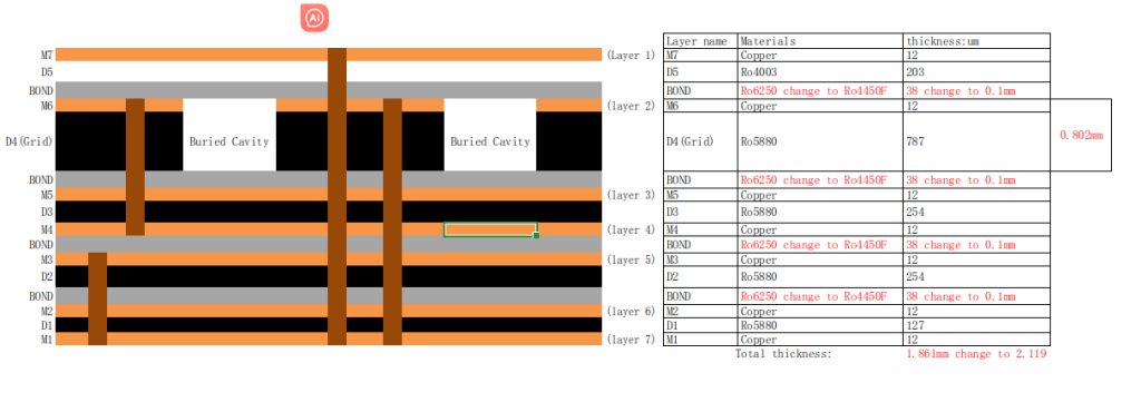
Das charakteristischste Merkmal dieser Leiterplatten ist das Vorhandensein von Hohlräumen, die präzise in die Struktur des Boards integriert sind. Diese Hohlräume können in Tiefe und Form variieren, abhängig von den spezifischen Anforderungen der Anwendung. The design must ensure that the cavities do not compromise the structural integrity of the board while providing the desired electrical characteristics.
Die Aufrechterhaltung der Signalintegrität bei hohen Frequenzen ist eine zentrale Herausforderung beim PCB-Design. Hochfrequenz-Hohlraum-Leiterplatten sind darauf ausgelegt, Signalverluste zu minimieren, Spiegelung, und Verzerrung, Dadurch wird sichergestellt, dass die Signale auch bei sehr hohen Frequenzen sauber und präzise bleiben. Die Hohlräume können verwendet werden, um die Impedanz der Leiterbahnen zu steuern und empfindliche Komponenten von potenziellen Störquellen zu isolieren.
Hochfrequenzkomponenten können erhebliche Wärmemengen erzeugen, Dies muss bewältigt werden, um Leistungseinbußen oder Schäden an der Platine zu verhindern. Die Hohlräume in diesen Leiterplatten können so gestaltet werden, dass sie eine bessere Wärmeableitung ermöglichen, entweder durch die Bereitstellung von Platz für Kühlkörper oder durch die Verbesserung der Luftzirkulation um kritische Komponenten.
Hochfrequenz-Hohlraum-Leiterplatten werden häufig an die spezifischen Anforderungen der Anwendung angepasst. Diese Anpassung kann die Größe und Form der Hohlräume umfassen, die Anzahl der Schichten, die verwendeten Materialien, und das Routing von Spuren. Die Möglichkeit, die Platine exakt an die Anforderungen der Anwendung anzupassen, ist einer der Hauptvorteile der Verwendung von Hohlraum-Leiterplatten.
Die Wahl der Materialien ist entscheidend für die Leistung von Hochfrequenz-Hohlraum-Leiterplatten. Materialien mit geringem dielektrischen Verlust, hohe Wärmeleitfähigkeit, und stabile elektrische Eigenschaften werden typischerweise verwendet, um eine optimale Leistung bei hohen Frequenzen sicherzustellen. Zu den gängigen Materialien gehört PTFE (Polytetrafluorethylen), Rogers-Laminate, und keramikgefüllte Substrate.
Materialien, die in Hochfrequenz-Hohlraum-Leiterplatten verwendet werden
Die in Hochfrequenz-Hohlraum-Leiterplatten verwendeten Materialien werden auf der Grundlage ihrer Fähigkeit ausgewählt, die anspruchsvollen Anforderungen des Hochfrequenzbetriebs zu erfüllen:
Das Substratmaterial spielt eine entscheidende Rolle bei der Bestimmung der elektrischen Leistung der Platine. PTFE, allgemein bekannt unter dem Markennamen Teflon, ist aufgrund seiner niedrigen Dielektrizitätskonstante und seines geringen Verlustfaktors eine beliebte Wahl für Hochfrequenzanwendungen. Rogers-Materialien, wie die Serien RO4000 und RO3000, werden auch häufig wegen ihrer hervorragenden Hochfrequenzleistung und Stabilität verwendet.
Kupfer ist das Standardmaterial für die leitenden Schichten in Hochfrequenz-Hohlraum-Leiterplatten. Jedoch, für sehr hochfrequente Anwendungen, Um den Signalverlust weiter zu reduzieren, können alternative Materialien wie Silber oder Gold verwendet werden. Die Dicke der leitenden Schichten wird sorgfältig kontrolliert, um eine gleichmäßige Impedanz auf der gesamten Platine sicherzustellen.
Die dielektrischen Schichten in Hochfrequenz-Hohlraum-Leiterplatten sind so konzipiert, dass sie eine Isolierung zwischen den leitenden Schichten bieten und gleichzeitig geringe dielektrische Verluste gewährleisten. Diese Schichten bestehen typischerweise aus Materialien wie PTFE oder anderen verlustarmen Dielektrika, um eine minimale Signaldämpfung zu gewährleisten.
Je nach Anwendungsfall können die Hohlräume in der Leiterplatte mit unterschiedlichen Materialien gefüllt werden. In einigen Fällen, Die Hohlräume bleiben leer, um Luftspalte zu schaffen, die dabei helfen, die Impedanz bestimmter Leiterbahnen zu kontrollieren. In anderen Fällen, Die Hohlräume können mit dielektrischen Materialien gefüllt werden, um die Leistung zu verbessern oder Komponenten mechanisch zu stützen.
Die Oberflächenbeschaffenheit der Leiterplatte ist entscheidend, um eine zuverlässige Lötung zu gewährleisten und die Leiterbahnen vor Oxidation zu schützen. Zu den gängigen Ausführungen gehört ENIG (Chemisches Nickel-Immersionsgold), Silber, oder andere spezielle Beschichtungen, die den Signalverlust reduzieren und die Leistung bei hohen Frequenzen verbessern sollen.
Herstellungsprozess von Hochfrequenz-Hohlraum-Leiterplatten
Der Herstellungsprozess von Hochfrequenz-Hohlraum-Leiterplatten umfasst mehrere präzise Schritte, um sicherzustellen, dass die Hohlräume präzise in die Platine integriert werden, ohne deren Leistung oder Zuverlässigkeit zu beeinträchtigen:
Der Prozess beginnt mit dem Design und Layout der Leiterplatte, inklusive der genauen Spezifikation der Hohlräume. Zur Modellierung der Platine wird fortschrittliche CAD-Software verwendet, einschließlich der Platzierung von Hohlräumen, Komponenten, und Spuren. Das Design muss die Elektrik berücksichtigen, Thermal-, und mechanischen Anforderungen der Anwendung.
Jede Schicht der Leiterplatte, einschließlich der Schichten, die die Hohlräume bilden, wird separat gefertigt. Die Leitermuster werden auf das kupferkaschierte Laminat geätzt, und die dielektrischen Schichten werden gemäß den Designvorgaben vorbereitet.
Die Hohlräume entstehen während des Schichtherstellungsprozesses. Dies kann mit verschiedenen Techniken erfolgen, wie zum Beispiel Fräsen, Laserschnitt, oder Radierung, je nach Größe, Form, und Tiefe des Hohlraums. Die Präzision dieses Prozesses ist entscheidend, um sicherzustellen, dass die Hohlräume den Designspezifikationen entsprechen, ohne die umgebenden Schichten zu beschädigen.
Die einzelnen Schichten werden gestapelt und unter Hitze und Druck zusammenlaminiert, um die endgültige Leiterplattenstruktur zu bilden. Der Laminierungsprozess muss sorgfältig kontrolliert werden, um sicherzustellen, dass die Hohlräume richtig ausgerichtet sind und die Platte flach und stabil bleibt.
Vias werden gebohrt, um verschiedene Schichten der Leiterplatte zu verbinden, und die Kavitäten werden für die Bauteilbestückung oder Weiterverarbeitung vorbereitet. Die Durchkontaktierungen und freiliegenden leitenden Bereiche werden dann mit zusätzlichem Kupfer oder anderen Metallen plattiert, um zuverlässige elektrische Verbindungen zu gewährleisten.
Die letzten Schritte umfassen das Aufbringen der Oberflächenveredelung auf die Leiterplatte und die Durchführung strenger Tests, um sicherzustellen, dass die Leiterplatte alle Leistungsspezifikationen erfüllt. Die Prüfung umfasst elektrische Prüfungen, Impedanzmessung, und Inspektion auf Mängel wie Fehlausrichtung oder Kurzschlüsse.
Anwendungen von Hochfrequenz-Hohlraum-Leiterplatten
Hochfrequenz-Hohlraum-Leiterplatten werden in einer Vielzahl von Anwendungen eingesetzt, bei denen es auf hohe Leistung und Zuverlässigkeit ankommt:
Diese Leiterplatten werden häufig in HF- und Mikrowellen-Kommunikationssystemen verwendet, einschließlich Mobilfunk-Basisstationen, Satellitenkommunikationsausrüstung, und Radarsysteme. Die Hohlräume ermöglichen die Integration von Hochfrequenzkomponenten, wie Filter und Verstärker, direkt in die Leiterplatte.
In Luft- und Raumfahrt- und Verteidigungsanwendungen, Hochfrequenz-Hohlraum-Leiterplatten werden in Systemen wie Radar verwendet, elektronische Kriegsführung, und Avionik. Die Fähigkeit, die Signalintegrität aufrechtzuerhalten und rauen Umgebungen standzuhalten, macht diese Leiterplatten ideal für geschäftskritische Anwendungen.
Hochfrequenz-Hohlraum-Leiterplatten werden auch in modernen medizinischen Geräten verwendet, wie Bildgebungssysteme und Diagnosegeräte, wo es auf Präzision und Zuverlässigkeit ankommt. Die Hohlräume ermöglichen die Integration spezieller Komponenten, die die Leistung des Geräts verbessern.
In der Automobilindustrie, Hochfrequenz-Hohlraumplatinen werden in fortschrittlichen Fahrerassistenzsystemen eingesetzt (Adas), Radar, und Kommunikationssysteme. Diese Platinen ermöglichen die Integration von Hochfrequenzkomponenten in kompakte und zuverlässige Systeme.
Vorteile von Hochfrequenz-Hohlraum-Leiterplatten
Hochfrequenz-Hohlraum-Leiterplatten bieten mehrere Vorteile, die sie in Hochleistungsanwendungen unverzichtbar machen:
Die Hohlräume helfen, die Impedanz zu kontrollieren und Signalverluste zu reduzieren, Dadurch wird sichergestellt, dass Hochfrequenzsignale mit minimaler Verzerrung oder Dämpfung übertragen werden.
Die Möglichkeit, Wärmemanagementfunktionen in die Hohlräume zu integrieren, ermöglicht eine bessere Wärmeableitung, Schutz empfindlicher Komponenten vor Überhitzung und Verbesserung der Gesamtzuverlässigkeit der Leiterplatte.
Die Flexibilität, Hohlräume entsprechend spezifischer Anwendungsanforderungen zu entwerfen, ermöglicht eine stärkere Anpassung und Optimierung der Leiterplatte für die Hochfrequenzleistung.
Durch die Integration von Hochfrequenzkomponenten direkt in die Leiterplatte, Hochfrequenz-Hohlraum-Leiterplatten reduzieren den Bedarf an externen Komponenten, Dies führt zu kompakteren und effizienteren Designs.
FAQ
Welche Arten von Bauteilen können in die Hohlräume einer Hochfrequenz-Leiterplatte integriert werden??
Komponenten wie Filter, Verstärker, Antennen, und Oszillatoren können in die Hohlräume einer Hochfrequenz-Leiterplatte integriert werden. Diese Hohlräume ermöglichen eine präzise Steuerung der elektrischen Eigenschaften, Verbesserung der Leistung dieser Hochfrequenzkomponenten.
Wie bewältigen Hochfrequenz-Hohlraum-Leiterplatten thermische Probleme??
Hochfrequenz-Hohlraum-Leiterplatten bewältigen thermische Probleme durch den Einbau von Hohlräumen, die Kühlkörper aufnehmen oder den Luftstrom um Hochfrequenzkomponenten verbessern können. Zusätzlich, Um die Wärmeableitung zu verbessern, können Materialien mit hoher Wärmeleitfähigkeit verwendet werden.
Welche Schlüsselfaktoren sind beim Entwurf einer Hochfrequenz-Hohlraum-Leiterplatte zu berücksichtigen??
Zu den wichtigsten zu berücksichtigenden Faktoren gehören die dielektrischen Eigenschaften der Materialien, die Präzision des Hohlraumdesigns, die Weiterleitung hochfrequenter Signale, und die Anforderungen an das Wärmemanagement. Die richtige Berücksichtigung dieser Faktoren gewährleistet eine optimale Leistung bei hohen Frequenzen.
Können Hochfrequenz-Hohlraum-Leiterplatten in rauen Umgebungen eingesetzt werden??
Ja, Hochfrequenz-Hohlraum-Leiterplatten sind oft so konzipiert, dass sie rauen Umgebungen standhalten, wie sie beispielsweise in Luft- und Raumfahrt- und Verteidigungsanwendungen zu finden sind. Die in diesen Leiterplatten verwendeten Materialien und Designtechniken stellen sicher, dass sie unter extremen Bedingungen zuverlässig funktionieren, einschließlich hoher Temperaturen und mechanischer Beanspruchung.