CO.,LTD")
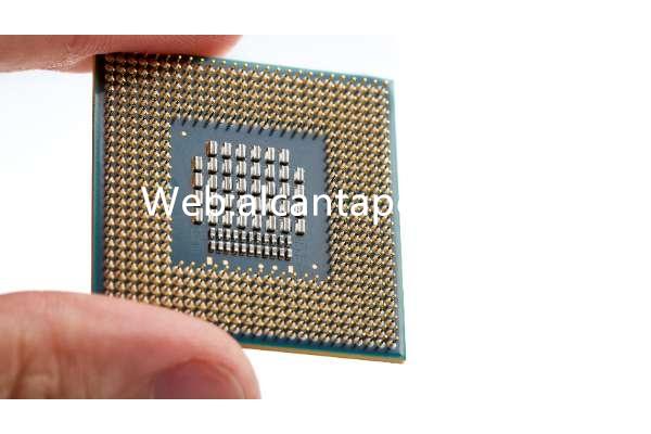
Mikrowelle/Mikrospur Leiterplatte Hersteller. HDI-Leiterplatten, und Lieferant von BGA-Gehäusesubstraten, die HDI-Vorstände und PaketsubstratSie werden aus Hochgeschwindigkeits- und Hochfrequenzmaterialien oder anderen Grundmaterialien hergestellt.
Im heutigen digitalen Zeitalter, Leiterplatte (Leiterplatte) ist zum Kernbestandteil fast aller elektronischen Geräte geworden. Die Entwicklung der Herstellungstechnologie für Mikrowellen-/Mikrotrace-Leiterplatten ist besonders wichtig für die drahtlose Kommunikation, Hochfrequenztechnik, und Hochfrequenz-Mikrowellenanwendungen. Dieser Artikel vermittelt Ihnen ein tiefgreifendes Verständnis der PCB-Definition, Design, Materialien, Herstellungsprozesse, Anwendungsbereiche, Vorteile, und Antworten auf Ihre häufig gestellten Fragen.
Was ist Mikrowellen-/Microtrace-PCB??
Mikrowellen-/Mikrospur-Leiterplatte, das heißt, Mikrowellen-/Mikrospuren-Leiterplatte, ist eine Leiterplatte, die speziell für Hochfrequenz-Mikrowellenanwendungen entwickelt wurde. Verglichen mit herkömmlichen Druckschaltplatten, Mikrowellen-/Microtrace-Leiterplatten sind strenger in Design und Herstellung, Sein Hauptzweck besteht darin, eine stabile Übertragung von Hochfrequenzsignalen und eine gute Impedanzanpassung sicherzustellen.
Der Entwurfs- und Herstellungsprozess von Mikrowellen-/Mikroleiterplatten ist komplex und erfordert viele besondere Überlegungen, um den Anforderungen von Hochfrequenz-Mikrowellenanwendungen gerecht zu werden. Erste, Designer müssen auf die Optimierung des Schaltungslayouts achten, um Signalübertragungsverluste und Interferenzen zu minimieren. Zusätzlich, Microtrace PCB erfordert auch die Verwendung von Mikrodrähten (Mikrospuren), die meist sehr feine Abmessungen haben und bestimmte Parameter wie Widerstand erfordern, Kapazität, und Induktivität. Das Design solch winziger Drähte erfordert präzise Berechnungen und fortschrittliche Fertigungstechniken, um eine stabile Leistung in Hochfrequenzumgebungen zu gewährleisten.
Während des Herstellungsprozesses, Mikrowellen-/Mikrospur-Leiterplatten verwenden häufig dielektrische Hochfrequenzmaterialien wie Polytetrafluorethylen (PTFE) um gute Isolationseigenschaften und geringe Verluste zu gewährleisten. Hersteller müssen außerdem fortschrittliche Bildgebungstechnologie und präzise chemische Verarbeitung nutzen, um mikroskopisch kleine Drähte und Details herzustellen, um die Leistung und Zuverlässigkeit der Leiterplatte sicherzustellen. Während der Montage, Besonderes Augenmerk muss auf die Handhabung und den Schutz der empfindlichen Drähte gelegt werden, um Schäden und Leistungseinbußen zu vermeiden.
Mikrowellen-/Microtrace-Leiterplatten werden häufig in vielen Hochfrequenz-Mikrowellenanwendungen eingesetzt, einschließlich Kommunikation, Radar, Satellitenkommunikation, drahtlose Netzwerke, medizinische Ausrüstung, und mehr. Seine hervorragende Leistung und Stabilität machen es zu einem unverzichtbaren Bestandteil in diesen Bereichen. Mit der richtigen Konstruktion und Herstellung, Mikrowellen-/Microtrace-Leiterplatten können einen höheren Frequenzgang erzielen, geringerer Übertragungsverlust und bessere Signalstabilität, Damit leisten sie einen wichtigen Beitrag zur Verbesserung der Leistung von Hochfrequenz-Mikrowellensystemen.
Zusamenfassend, Mikrowellen-/Microtrace-Leiterplatten spielen eine entscheidende Rolle bei Hochfrequenz-Mikrowellenanwendungen. Die kontinuierliche Weiterentwicklung seiner Design- und Fertigungstechnologie wird den Herstellern elektronischer Geräte innovativere Lösungen bieten und die Entwicklung und Weiterentwicklung der Hochfrequenz-Mikrowellentechnologie fördern. Anwendung.
Referenzhandbuch zum Mikrowellen-/Mikrospuren-PCB-Design.
Der Schlüssel zur Herstellung von Mikrowellen-/Mikrotrace-Leiterplatten ist das Design. In diesem Design-Referenzhandbuch, Wir werden uns mit den Schlüsselfaktoren für eine stabile Signalübertragung und eine gute Impedanzanpassung befassen.
Erste, Der Designprozess muss die Besonderheiten von Mikrowellen- und Hochfrequenzsignalen vollständig berücksichtigen. Denn diese Signale haben höhere Frequenzen und kürzere Wellenlängen, Die Länge und Anordnung der Übertragungsleitungen sind entscheidend für die Übertragungsleistung des Signals. daher, beim Entwurf der Leiterplattenverkabelung, Es ist notwendig, geeignete Übertragungsleitungstypen zu übernehmen (wie Mikrostreifenleitungen oder Koaxialleitungen) und optimierte Layout-Schemata, um eine stabile Signalübertragung und minimalen Signalverlust zu gewährleisten.
Zweitens, Die Impedanzanpassung ist der Schlüssel für eine gute Signalübertragung. Bei der Herstellung von Mikrowellen-/Microtrace-Leiterplatten ist häufig eine strenge Impedanzkontrolle erforderlich, um die Signalimpedanzanpassung im gesamten Schaltkreis sicherzustellen. Während des Designprozesses, Um das Impedanzanpassungsschema zu simulieren und zu optimieren, um den Anforderungen spezifischer Anwendungen gerecht zu werden, sind hochpräzise Berechnungstools und Simulationssoftware erforderlich.
Zusätzlich zu Routing und Impedanzanpassung, Es sind noch weitere Schlüsselfaktoren zu berücksichtigen, wie etwa elektromagnetische Verträglichkeit (EMV), Wärmemanagement, und Zuverlässigkeit. Bei der Herstellung von Mikrowellen-/Mikrospur-Leiterplatten müssen diese Faktoren während der Entwurfsphase vollständig berücksichtigt werden, um die Leistung und Zuverlässigkeit des Endprodukts sicherzustellen.
Endlich, Professionelle Designleitfäden bieten Ihnen detaillierte Anleitungen, die Ihnen helfen, die neuesten Designtechniken und Best Practices zu verstehen und anzuwenden. Diese Leitfäden enthalten in der Regel Designspezifikationen, Layout-Empfehlungen, Anforderungen an die Impedanzkontrolle, und FAQs, um Ihnen umfassende Designunterstützung und technische Anleitung zu bieten.
Um zusammenzufassen, Beim Mikrowellen-/Mikrotrace-PCB-Design müssen Faktoren wie die Verkabelung umfassend berücksichtigt werden, Impedanzanpassung, elektromagnetische Verträglichkeit, usw., um sicherzustellen, dass das Endprodukt eine stabile Signalübertragungsleistung und hervorragende elektrische Eigenschaften aufweist. Durch professionelle Design-Guides, Sie können die neueste Designtechnologie besser verstehen und anwenden, Bereitstellung umfassender technischer Unterstützung und Anleitung für Ihr PCB-Design.
Welches Material wird in Mikrowellen-/Mikrotrace-Leiterplatten verwendet??
Die bei der Herstellung von Mikrowellen-/Mikrotrace-Leiterplatten verwendeten Materialien sind einer der Schlüsselfaktoren, die sich direkt auf die Leistung im Hochfrequenz-Mikrowellenfeld auswirken. In diesem Bereich, Dabei spielen hochfrequente dielektrische Materialien eine entscheidende Rolle, und PTFE (Polytetrafluorethylen) ist eine beliebte Wahl. PTFE verfügt über hervorragende dielektrische Eigenschaften und eine stabile Chemie, Dies ermöglicht eine gute Leistung in Hochfrequenzumgebungen. Es hat die Eigenschaften eines geringen Verlusts, niedrige Dielektrizitätskonstante und niedriger dielektrischer Verlustfaktor, wodurch der Energieverlust bei der Signalübertragung wirksam reduziert werden kann, Dadurch wird die Übertragungseffizienz verbessert.
Zusätzlich zu PTFE, Ein weiteres häufig verwendetes dielektrisches Hochfrequenzmaterial ist FR-4. Obwohl FR-4 hauptsächlich für die allgemeine Leiterplattenherstellung verwendet wird, Es kann auch für die Herstellung von Microtrace-Leiterplatten in einigen spezifischen Hochfrequenzanwendungen verwendet werden. Es weist eine hohe mechanische Festigkeit und thermische Stabilität auf, und kann in bestimmten Situationen eine akzeptable Hochfrequenzleistung bieten.
Zusätzlich, Für die Herstellung von Mikroleiterplatten sind spezielle leitfähige Materialien erforderlich, um Präzisionsdrähte und Mikroleiterbahnen zu ermöglichen. Bei diesen leitfähigen Materialien handelt es sich üblicherweise um Metallfilme, wie Kupfer, Silber oder Gold, die eine hervorragende Leitfähigkeit und stabile Leiteigenschaften aufweisen, Gewährleistung einer präzisen Signalübertragung und einer guten Impedanzanpassung.
Im Allgemeinen, Die bei der Herstellung von Mikrowellen-/Mikrotrace-Leiterplatten verwendeten Materialien müssen Hochfrequenzeigenschaften aufweisen, Stabilität, und geringem Verlust, um den strengen Anforderungen von Hochfrequenz-Mikrowellenumgebungen gerecht zu werden. Die Auswahl der richtigen Materialien ist entscheidend für die Gewährleistung der Leistung und Zuverlässigkeit von Leiterplatten, Dies ist einer der Gründe, warum Mikrowellen-/Microtrace-Leiterplatten in Hochfrequenz-Mikrowellenanwendungen beliebt sind.
Welche Größe haben Mikrowellen-/Mikrotrace-Leiterplatten??
Mikrowellen-/Microtrace-Leiterplatten sind in ihrer Größe äußerst flexibel und können an die Anforderungen einer bestimmten Anwendung angepasst werden. Die Mikrowellen-/Microtrace-PCB-Herstellungstechnologie ermöglicht komplexe Schaltungs- und Mikrodesigndesigns mit hoher Packungsdichte, hohe Leistungsanforderungen.
In vielen Hochfrequenz-Mikrowellenanwendungen, Kompakte Größe ist entscheidend. Mikrowellen-/Microtrace-Leiterplatten können extrem kleine Größen erreichen, So können sie mehr Funktionalität auf kompaktem Raum unterbringen. Zum Beispiel, in mobilen Kommunikationsgeräten, Satellitenkommunikationssysteme, und medizinische Diagnosegeräte, Um komplexe Funktionen umzusetzen und auf begrenztem Raum optimale Leistung zu erzielen, sind hochintegrierte Leiterplatten erforderlich.
Zusätzlich zur Größenminiaturisierung, Die Mikrowellen-/Microtrace-Leiterplattenfertigungstechnologie ermöglicht eine Verdrahtung mit hoher Dichte. Durch miniaturisiertes Schaltungsdesign und fortschrittliche Herstellungsprozesse, mehr Funktionen können in kleinere Leiterplatten integriert werden, Dadurch wird eine höhere Leistung und Funktionsdichte erreicht.
In einigen speziellen Anwendungen, wie der Luft- und Raumfahrtbereich und medizinische Geräte, Die Anforderungen an Leiterplattengröße und -gewicht sind sehr streng. Das miniaturisierte Design der Mikrowellen-/Microtrace-Leiterplatte kann dazu beitragen, das Gewicht und die Größe des Geräts zu reduzieren und gleichzeitig die Systemleistung und -zuverlässigkeit zu verbessern.
Zusamenfassend, Mit der Mikrowellen-/Microtrace-Leiterplattenfertigungstechnologie lässt sich nicht nur das Design komplexer Schaltkreise und winziger Größen realisieren, sondern erfüllen auch Anforderungen an hohe Dichte und Leistung. Seine Flexibilität und Anpassbarkeit machen es ideal für viele Hochfrequenz-Mikrowellenanwendungen.
Der Herstellungsprozess von Mikrowellen-/Mikrospur-Leiterplatten.
Der Herstellungsprozess von Mikrowellen-/Mikrotrace-Leiterplatten ist ein komplexer und präziser Prozess, unter Einbeziehung einer Vielzahl von Schlüsseltechnologien und Verknüpfungen. Vom Entwurf bis zum fertigen Produkt, Eine strenge Qualitätskontrolle und professionelle technische Unterstützung sind erforderlich.
Erstens, Design spielt eine Schlüsselrolle im Herstellungsprozess von Mikrowellen-/Mikrotrace-Leiterplatten. Das Designteam muss das Schaltungslayout und die Verkabelung basierend auf den Anforderungen der spezifischen Anwendung und unter Berücksichtigung der Eigenschaften hochfrequenter Mikrowellensignale entwerfen. Mithilfe fortschrittlicher CAD-Software erstellen sie Konstruktionszeichnungen, um eine Impedanzanpassung der Schaltung und eine stabile Signalübertragung sicherzustellen.
Anschließend, Der Herstellungsprozess umfasst die Vorbereitung des Substrats. Nach Auswahl des geeigneten Untergrundmaterials, Um eine gute Haftung und Leitfähigkeit zu gewährleisten, werden chemische Verarbeitungstechniken eingesetzt, um die Substratoberfläche zu behandeln. Zu diesen chemischen Behandlungen gehört die Reinigung, Oxidentfernung, und Anpassung der Oberflächenrauheit als Vorbereitung für die anschließende Strukturierung.
Nächste, Bildgebungstechnologie wird verwendet, um Mikromuster von Microtrace-Leiterplatten zu erstellen. Verwendung der Fotolithografie-Technologie, Das Designmuster wird auf die Oberfläche des Substrats übertragen, und das erforderliche Schaltkreismuster wird durch die Einwirkung von Photosensibilisator und ultraviolettem Licht gebildet. Dieser Schritt erfordert hochentwickelte Ausrüstung und präzise Vorgänge, um die Genauigkeit und Klarheit des Musters sicherzustellen.
Die strukturierte Substratoberfläche wird dann mithilfe chemischer Ätz- oder Metallabscheidungstechniken bearbeitet. Ein Stromkreis wird durch Ätzen oder Abscheiden von Metall vervollständigt, um leitende Pfade und Verbindungen zu schaffen. In diesem Prozess, Eine strenge Prozesskontrolle und eine präzise Parametereinstellung sind entscheidend, um die Qualität und Stabilität der Schaltung sicherzustellen.
Endlich, nach Inspektion und Prüfung, Die Microtrace-Leiterplatte tritt in die nächste Phase der Montage und Verpackung ein. Während des gesamten Herstellungsprozesses werden strenge Qualitätskontrollverfahren und professionelle technische Unterstützung implementiert, um sicherzustellen, dass das Endprodukt den Designanforderungen und Kundenerwartungen entspricht.
Um zusammenzufassen, Der Herstellungsprozess von Mikrowellen-/Mikrotrace-Leiterplatten ist ein präziser und komplexer Prozess, der eine Vielzahl von Schlüsseltechnologien und Verbindungen umfasst. Durch hervorragende Technologie und strenge Qualitätskontrolle, Wir können Höchstleistungen erbringen, zuverlässige Microtrace-PCB-Produkte, die den Anforderungen verschiedener Hochfrequenz-Mikrowellenanwendungen gerecht werden.
Der Anwendungsbereich von Mikrowellen-/Mikrospur-Leiterplatten.
Die Mikrowellen-/Mikrospur-Leiterplattenherstellungstechnologie wird häufig in Bereichen wie der Kommunikation eingesetzt, Radar, Satelliten, und medizinische Geräte. Seine Hochfrequenzeigenschaften und seine stabile Leistung machen es zur ersten Wahl für viele kritische Anwendungen.
Im Bereich Kommunikation, Mikrowellen-/Microtrace-Leiterplatten werden häufig in drahtlosen Kommunikationsgeräten verwendet, Basisstationen und Netzwerkausrüstung. Mit der Weiterentwicklung der 5G-Technologie, Mikrowellen-/Microtrace-PCBs bieten zuverlässige Lösungen für die effiziente Nutzung von Spektrumressourcen und Anforderungen an eine schnelle und stabile Signalübertragung. Sie sorgen für eine stabile Übertragungsleistung bei hohen Frequenzen, Sicherstellung der Qualität und Zuverlässigkeit von Kommunikationssignalen.
Radarsysteme sind ebenfalls einer der wichtigen Anwendungsbereiche von Mikrowellen-/Mikrotrace-Leiterplatten. Radarsysteme benötigen zur Erkennung und Messung hochfrequente Mikrowellensignale, Die Design- und Fertigungskapazitäten von Microtrace PCB können die Anforderungen des Radarsystems an eine präzise Signalverarbeitung und -übertragung erfüllen. Vom militärischen Einsatz bis hin zu zivilen Anwendungen, Die Entwicklung von Radarsystemen ist untrennbar mit der Unterstützung der Mikrowellen-/Microtrace-PCB-Technologie verbunden.
Im Satellitenbereich, Mikrowellen-/Mikrospur-Leiterplatten werden häufig in der Satellitenkommunikation eingesetzt, Navigations- und Fernerkundungssysteme. Satelliten erfordern einen langfristig stabilen Betrieb unter extremen Umweltbedingungen, Die Hochfrequenzeigenschaften und die stabile Leistung von Microtrace PCB machen es zur idealen Wahl für Satellitensysteme. Sie sind in der Lage, unter extremen Bedingungen wie hohen Temperaturen eine gute Leistung aufrechtzuerhalten, niedrige Temperaturen und Strahlung im Weltraum.
Zusätzlich, im Bereich medizinischer Geräte, Auch Mikrowellen-/Microtrace-Leiterplatten spielen eine wichtige Rolle. Medizinische Geräte stellen sehr hohe Anforderungen an die Stabilität und Genauigkeit der Signalübertragung, insbesondere bei medizinischen Bildgebungs- und Diagnosegeräten. Die Hochfrequenzeigenschaften und die Zuverlässigkeit von Microtrace PCB machen es zu einem unverzichtbaren Bestandteil verschiedener medizinischer Geräte, Bereitstellung zuverlässiger technischer Unterstützung für medizinische Diagnose und Behandlung.
Gesamt, Das breite Anwendungsspektrum der Mikrowellen-/Mikrospur-PCB-Herstellungstechnologie erstreckt sich über viele Schlüsselbereiche, einschließlich Kommunikation, Radar, Satelliten, und medizinische Geräte. Seine Hochfrequenzeigenschaften, Stabile Leistung und Zuverlässigkeit machen es zur ersten Wahl für verschiedene kritische Anwendungen, und spielt eine wichtige Rolle bei der Förderung der Entwicklung moderner Wissenschaft und Technologie sowie Anwendungsinnovationen.
Was sind die Vorteile von Mikrowellen-/Microtrace-PCB??
Die Mikrowellen-/Microtrace-Leiterplattenherstellungstechnologie bietet im Hochfrequenz-Mikrowellenbereich offensichtliche Vorteile gegenüber herkömmlichen Leiterplatten. Nachfolgend finden Sie eine detaillierte Beschreibung dieser Vorteile:
Geringerer Übertragungsverlust
In Hochfrequenz-Mikrowellenanwendungen, Der Signalübertragungsverlust ist ein entscheidender Faktor. Die Mikrowellen-/Microtrace-PCB-Herstellungstechnologie nutzt hochfrequente dielektrische Materialien und präzise Verarbeitungstechnologie, um den Energieverlust während der Signalübertragung wirksam zu reduzieren, Dadurch wird die Signalstabilität und -zuverlässigkeit gewährleistet.
Bessere Impedanzanpassung
In Hochfrequenz-Mikrowellensystemen, Die Impedanzanpassung ist entscheidend für die Stabilität der Signalübertragung. Mit der Mikrowellen-/Microtrace-PCB-Herstellungstechnologie kann eine präzise Impedanzsteuerung erreicht und die Signalanpassungsleistung im gesamten Schaltkreis sichergestellt werden, Dadurch werden Signalreflexion und -verlust reduziert und die Systemleistung und -effizienz verbessert.
Höherer Frequenzgang
Hochfrequenz-Mikrowellenanwendungen stellen sehr strenge Anforderungen an den Frequenzgang, und herkömmliche Leiterplatten können bei hohen Frequenzen unter Signaldämpfung und Verzerrung leiden. Die Herstellungstechnologie für Mikrowellen-/Microtrace-Leiterplatten verwendet hochfrequente dielektrische Materialien und ein präzises Schaltungsdesign, um einen höheren Frequenzgangbereich und eine bessere Signalübertragungsleistung zu erreichen, Erfüllung der Frequenzganganforderungen von Hochfrequenz-Mikrowellensystemen.
Höhere Zuverlässigkeit
In Hochfrequenz-Mikrowellenanwendungen, Die Systemzuverlässigkeit ist für den stabilen Betrieb der Geräte von entscheidender Bedeutung. Die Mikrowellen-/Microtrace-PCB-Herstellungstechnologie verwendet hochwertige Materialien und strenge Herstellungsprozesse, um die Stabilität und Zuverlässigkeit von PCBs zu gewährleisten. Im Vergleich zu herkömmlichen Leiterplatten, Mikrowellen-/Microtrace-Leiterplatten haben eine bessere Hochtemperaturbeständigkeit, hohe Druckfestigkeit und Anti-Interferenz-Fähigkeiten, und kann in rauen Umgebungen über einen langen Zeitraum stabil betrieben werden.
Gesamt, Die Mikrowellen-/Microtrace-PCB-Herstellungstechnologie schneidet im Hochfrequenz-Mikrowellenbereich gut ab. Seine hervorragende Übertragungsleistung, Präzise Impedanzkontrolle, Breiter Frequenzgang und hohe Zuverlässigkeit machen es zur ersten Wahl für viele Hochfrequenz-Mikrowellenanwendungen. planen. Ob im Bereich Kommunikation, Radar, Satelliten oder medizinische Geräte, Wenn Sie sich für die Mikrowellen-/Microtrace-Leiterplattenfertigungstechnologie entscheiden, können Sie Ihren Produkten höhere Leistungs- und Zuverlässigkeitsgarantien bieten.
FAQ
Für welche Frequenzbereiche sind Mikrowellen-/Microtrace-Leiterplatten geeignet??
Die Mikrowellen-/Microtrace-Leiterplattenfertigungstechnologie ist für einen breiten Frequenzbereich geeignet, Die Bandbreite reicht von einigen hundert Megahertz bis hin zu mehreren zehn Gigahertz. Dadurch wird es häufig in Hochfrequenz-Mikrowellenanwendungen eingesetzt, einschließlich Kommunikation, Radar, Satellitenkommunikation und andere Felder. Aufgrund der strengeren Design- und Fertigungsanforderungen, Mikrowellen-/Microtrace-PCBs können in Hochfrequenzumgebungen für geringere Übertragungsverluste und eine bessere Impedanzanpassung sorgen, Dadurch wird die Stabilität und Leistung des Systems gewährleistet.
Wie lange dauert die Herstellung von Mikrowellen-/Mikrotrace-Leiterplatten??
Die Zykluszeiten für die Herstellung von Mikrowellen-/Mikrospur-Leiterplatten hängen von der spezifischen Komplexität des Designs ab, Materialauswahl, und Herstellerfähigkeiten und -ressourcen. Allgemein gesprochen, Die Vorlaufzeit von der Designbestätigung bis zur Lieferung des fertigen Produkts beträgt in der Regel einige Tage bis einige Wochen. Für einfache Designs und häufig verwendete Materialien, Die Herstellungszyklen können kürzer sein; für komplexe Hochfrequenz-Mikrowellendesigns, Es kann länger dauern, bis Qualität und Leistung gewährleistet sind. daher, bei der Auswahl eines Leiterplattenherstellers, Es wird empfohlen, mit ihnen eine klare Vorlaufzeit zu vereinbaren, damit Ihr Projekt pünktlich abgeschlossen werden kann.
Wie viel kostet eine Mikrowellen-/Microtrace-Leiterplatte??
Die Kosten einer Mikrowellen-/Mikrotrace-Leiterplatte hängen von mehreren Faktoren ab, einschließlich Designkomplexität, Materialauswahl, Herstellungsprozess, und Auftragsvolumen. Die Herstellung von Mikrowellen-/Mikrospur-Leiterplatten ist in der Regel mit höheren Kosten verbunden als die herkömmliche Leiterplattenherstellung, vor allem aufgrund der dafür erforderlichen hochwertigen Materialien und Präzisionsfertigungsprozesse. Jedoch, angesichts seiner hervorragenden Leistung und Stabilität bei Hochfrequenz-Mikrowellenanwendungen, sowie seine erheblichen Auswirkungen auf die Systemleistung, Die Kosten für Mikrowellen-/Mikrotrace-Leiterplatten lohnen sich oft. Bei der Auswahl eines Leiterplattenherstellers, Sie können Ihre Projektanforderungen und Ihr Budget bewerten, um die am besten geeignete Lösung zu finden.
Was ist der Unterschied zwischen Mikrowellen-/Mikrotrace-Leiterplatten und herkömmlichen Leiterplatten??
Mikrowellen-/Microtrace-Leiterplatten unterscheiden sich im Design deutlich von herkömmlichen Leiterplatten, Materialauswahl und Herstellungsprozesse. Erste, Mikrowellen-/Microtrace-Leiterplatten sind speziell für Hochfrequenz-Mikrowellenanwendungen konzipiert, die hochwertigere Materialien und präzisere Herstellungsprozesse erfordern. Zweitens, Mikrowellen-/Microtrace-Leiterplatten stellen besondere Anforderungen an die Verkabelung, Layout und Impedanzanpassung sorgen für eine stabile Übertragung und Leistung von Hochfrequenzsignalen. daher, im Vergleich zu herkömmlichen Leiterplatten, Mikrowellen-/Microtrace-Leiterplatten eignen sich besser für Anwendungsszenarien mit höheren Signalqualitäts- und Leistungsanforderungen, wie zum Beispiel Kommunikation, Radar- und Satellitenkommunikation.