КОМПАНИЯ С ОГРАНИЧЕННОЙ ОТВЕТСТВЕННОСТЬЮ")
Производитель печатных плат с радиочастотными полостями. Производитель печатных плат с радиочастотными полостями специализируется на изготовлении сложных печатных плат. (печатные платы) оптимизирован для радиочастотных приложений. Эти печатные платы тщательно разработаны для размещения радиочастотных резонаторов., обеспечение эффективной передачи сигнала и минимальных помех. Использование передовых технологий и точного проектирования., они создают платы, адаптированные к точным спецификациям радиочастотных систем., обслуживание таких отраслей, как телекоммуникации, аэрокосмический, и медицинское оборудование. С акцентом на качество и производительность, их опыт заключается в производстве печатных плат, обеспечивающих бесперебойную связь и надежную работу в высокочастотных средах., отвечающее требованиям современных беспроводных технологий.
В области современной электроники, с быстрым развитием высокочастотный электронное оборудование и системы, Печатная плата с радиочастотным резонатором стала одним из незаменимых основных компонентов. В этой статье мы углубимся в принципы проектирования., производственные процессы и широкий спектр применения радиочастотного резонатора печатная плата, Целью является предоставление читателям комплексного руководства, которое поможет им лучше понять эту ключевую технологию и изучить перспективы ее применения в будущем..
Что такое печатная плата с радиочастотным резонатором?
Печатная плата с радиочастотным резонатором представляет собой специально разработанную печатную плату, предназначенную для высокочастотного электронного оборудования.. В конструкции печатной платы с радиочастотным резонатором, характеристики высокочастотных электромагнитных волн принимаются во внимание для обеспечения стабильной передачи сигнала и электромагнитных характеристик в высокочастотных средах.. По сравнению с традиционными печатными платами, В печатной плате с радиочастотным резонатором используются специальные материалы и процессы для удовлетворения требований целостности сигнала и электромагнитной совместимости высокочастотного электронного оборудования..
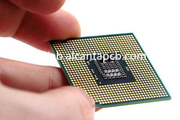
Особенностью печатной платы с радиочастотным резонатором является ее полостная структура и металлизация.. Структура полости эффективно изолирует электромагнитные волны., уменьшает помехи сигнала и перекрестные помехи, и повышает стабильность и надежность передачи сигнала. Обработка металлизацией может эффективно улучшить проводящие характеристики печатной платы., уменьшить потери и отражение сигнала, и обеспечить быструю передачу сигналов в высокочастотной среде.
Для удовлетворения требований высокочастотного электронного оборудования, В печатной плате с радиочастотным резонатором обычно используются высокоэффективные диэлектрические материалы., например, ПТФЭ (политетрафторэтилен) и RO4003C (армированный стекловолокном ПТФЭ). Эти материалы имеют низкие потери., низкая диэлектрическая проницаемость и стабильные диэлектрические свойства, и может поддерживать низкие потери и искажения при передаче сигнала в высокочастотных средах.
Кроме того, Процесс производства печатной платы с радиочастотным резонатором также относительно сложен.. В процессе производства, точное ламинирование, конструкция полости, и металлизация необходимы для обеспечения стабильности работы печатной платы в высокочастотных средах.. Высокочастотные среды предъявляют более высокие требования к процессу изготовления печатных плат., требующее точного оборудования и контроля процесса для обеспечения качества и надежности печатных плат..
Общий, Печатная плата с радиочастотным резонатором играет жизненно важную роль в высокочастотном электронном оборудовании.. Они могут не только соответствовать строгим требованиям к передаче сигналов и электромагнитным характеристикам высокочастотного электронного оборудования., но также обеспечить стабильные и надежные решения, оказание важной поддержки развитию современных коммуникаций, радиолокационные системы, спутниковая связь и другие области.
Справочное руководство по проектированию печатной платы с радиочастотным резонатором.
Печатная плата с радиочастотным резонатором (Печатная плата с радиочастотным резонатором) это печатная плата, специально разработанная для высокочастотного электронного оборудования.. Его уникальная структура и выбор материалов позволяют ему поддерживать стабильную передачу сигнала и электромагнитные характеристики в высокочастотных средах.. В этом руководстве будут рассмотрены основы проектирования печатных плат с радиочастотным резонатором., помогая читателям понять, как эффективно проектировать и производить эту важную высокочастотную печатную плату..
Проектирование печатной платы с радиочастотным резонатором требует учета многих факторов., включая частотную характеристику, целостность сигнала, электромагнитная совместимость, термоменеджмент и технология упаковки. Первый, проектировщикам необходимо иметь глубокое понимание частотных характеристик схемы, чтобы гарантировать, что схема может стабильно работать в расчетном диапазоне частот.. Во-вторых, разумная компоновка и конструкция цепи имеют решающее значение для снижения потерь при передаче сигнала и электромагнитных помех.. Кроме того, для мощного и высокочастотного оборудования, хорошая конструкция управления температурным режимом также необходима, чего можно достичь за счет оптимизации конструкции рассеивания тепла и выбора соответствующих материалов рассеивания тепла..
В процессе производства, Требования к производственному процессу для печатных плат с радиочастотным резонатором более строгие.. Прежде всего, Точный процесс ламинирования и конструкция полости могут обеспечить высокочастотные характеристики и электромагнитные характеристики печатной платы.. Во-вторых, Выбор металлизации и высокочастотных материалов имеет решающее значение для улучшения проводимости цепи и снижения потерь при передаче.. Кроме того, для высокочастотных плат, требования к контролю расстояния между досками и плоскостности поверхности выше, требующие использования современного технологического оборудования и контроля процесса..
Печатная плата с радиочастотной полостью широко используется в беспроводной связи., радиолокационные системы, спутниковая связь, радиочастотная идентификация (RFID) и другие поля. В этих приложениях, Печатная плата с радиочастотной полостью может не только обеспечивать высокочастотную производительность., но также удовлетворить потребности в обработке и передаче сигналов сложных систем. Например, в системах беспроводной связи, Печатная плата с радиочастотной полостью может обеспечивать высокоскоростную передачу данных и подключение нескольких антенных систем., предоставление важной поддержки развитию технологий беспроводной связи.
По сравнению с традиционной конструкцией печатной платы, Печатная плата с радиочастотной полостью имеет лучшую защиту от помех, меньшие потери при передаче и более высокая частотная характеристика. Они также обеспечивают более компактную компоновку и более высокую интеграцию., предоставление более стабильного и надежного решения для высокочастотного электронного оборудования. С помощью этого руководства, Мы надеемся, что читатели смогут получить более полное представление о принципах проектирования и процессах производства печатных плат с радиочастотным резонатором., предоставить ссылки на исследования и применения в смежных областях, и способствовать развитию и применению высокочастотных электронных технологий..
Какой материал используется в печатной плате с радиочастотным резонатором??
Выбор материала печатной платы с радиочастотным резонатором имеет решающее значение и напрямую влияет на ее производительность и стабильность в высокочастотных средах.. Обычно используемые материалы включают в себя:
ПТФЭ (политетрафторэтилен): ПТФЭ — это материал с низкой диэлектрической проницаемостью и низкими тангенциальными потерями, обладающий превосходными высокочастотными характеристиками.. Он широко используется в радиочастотных приложениях и может эффективно снизить потери при передаче сигнала и повысить эффективность передачи сигнала..
Материал FR4: FR4 — это распространенный материал из эпоксидной смолы, армированный стекловолокном, который широко используется в производстве обычных печатных плат.. Хотя его характеристики в высокочастотной среде не так хороши, как у ПТФЭ., он по-прежнему имеет хорошие характеристики в диапазоне низких и средних частот, а стоимость относительно низкая..
Композитный материал из стекловолокна ПТФЭ: Этот материал сочетает в себе превосходные высокочастотные характеристики ПТФЭ с прочностью материалов, армированных стекловолокном., поэтому он широко используется в производстве печатных плат с радиочастотными полостями.. Имеет отличные диэлектрические свойства, тепловая стабильность и механическая прочность, и подходит для приложений с высокими требованиями к высокочастотным характеристикам и надежности..
Металлическая подложка: Для некоторых мощных радиочастотных приложений, требующих высокой эффективности рассеивания тепла и механической прочности., печатная плата с металлической подложкой стала опцией. Обычные металлические подложки включают алюминиевые и медные подложки., которые имеют превосходные свойства рассеивания тепла и механическую прочность и подходят для таких применений, как мощные усилители радиочастоты..
Керамические материалы: Для некоторых применений, требующих большего размера и веса, такие как оборудование мобильной связи и оборудование спутниковой связи, керамические материалы стали вариантом. Имеют отличные высокочастотные характеристики., стабильность размеров и устойчивость к высоким температурам, и подходят для высокопроизводительных, миниатюрные радиочастотные модули и компоненты.
Благодаря разумному выбору и дизайну материалов, Печатная плата с радиочастотным резонатором может обеспечить стабильную и надежную передачу сигнала и электромагнитные характеристики в высокочастотных средах., удовлетворение потребностей различных сценариев применения.
Какой размер печатной платы с радиочастотной полостью??
Размер печатной платы с радиочастотным резонатором обычно зависит от конкретного сценария и системных требований ее применения.. Из-за особенностей высокочастотных сигналов, Печатная плата с радиочастотным резонатором часто требует более точного проектирования и изготовления, чтобы обеспечить стабильную передачу сигнала и отличные электромагнитные характеристики..
Вообще говоря, Размер печатной платы с радиочастотным резонатором может удовлетворить различные потребности приложений от маленьких до больших. В малом форм-факторе, они могут быть интегрированы с микроволновыми радиочастотными устройствами, например, в мобильных телефонах, Беспроводное сетевое оборудование, или радиолокационные системы. Эти небольшие печатные платы с радиочастотным резонатором обычно требуют компактной компоновки и высокоинтегрированной конструкции, чтобы адаптироваться к тенденции миниатюризации оборудования..
По большому размеру, Печатная плата с радиочастотным резонатором может использоваться в более сложных системах, такие как базовые станции связи, наземные станции спутниковой связи или оборудование для медицинской визуализации. Эти печатные платы с большими радиочастотными полостями часто требуют больших площадей для размещения большего количества компонентов и соединений., и такие проблемы, как рассеивание тепла и электромагнитные помехи, также необходимо учитывать..
В дополнение к общему размерному ряду, форма печатной платы с радиочастотным резонатором также может варьироваться в зависимости от конкретного применения. Некоторые из них могут иметь обычный прямоугольный или квадратный дизайн., в то время как другим могут потребоваться нетрадиционные формы, такие как овалы или неправильные формы, в зависимости от конкретных требований к компоновке системы..
В общем, размер печатной платы радиочастотного резонатора разнообразен, в зависимости от сценария применения и системных требований. Будь то небольшое встроенное устройство или крупная коммуникационная инфраструктура, он может быть спроектирован индивидуально в соответствии с конкретными потребностями для достижения оптимальной производительности и надежности..
Процесс изготовления печатной платы с радиочастотным резонатором.
Процесс производства печатной платы с радиочастотным резонатором включает в себя несколько ключевых процессов., требующее прецизионного оборудования и строгого контроля процесса. Вот основные этапы процесса:
Во-первых, это прецизионный процесс ламинирования.. При изготовлении печатных плат с радиочастотными резонаторами, процесс ламинирования имеет решающее значение. Это включает в себя укладку нескольких слоев диэлектрических материалов и металлических слоев точно так, как задумано, и затвердевание их в одно целое с использованием высоких температур и давлений.. Это гарантирует, что межслойная диэлектрическая проницаемость и толщина печатной платы контролируются в пределах проектных спецификаций., тем самым обеспечивая производительность передачи сигнала в высокочастотной среде.
Во-вторых, конструкция полости. Для печатной платы с радиочастотной полостью обычно требуется полость внутри платы для герметизации высокочастотных цепей и обеспечения электромагнитного экранирования.. Эти полости требуют точного проектирования и изготовления для обеспечения стабильной электромагнитной среды в условиях высокочастотной эксплуатации..
Далее идет металлизация. При изготовлении печатных плат с радиочастотными резонаторами, необходима прецизионная металлизация на поверхности и внутренних металлических слоях печатной платы.. Это включает в себя гальваническое или химическое меднение для создания проводящих путей и слоев заземления для обеспечения соединения и экранирования цепи..
Выбор высокочастотного материала также является важнейшим звеном производственного процесса.. Выбор материалов, подходящих для высокочастотных применений, имеет решающее значение для производительности печатных плат с радиочастотными резонаторами.. Обычно используемые высокочастотные материалы включают политетрафторэтилен. (ПТФЭ), керамические подложки и полиимид (ПИ), которые имеют низкие диэлектрические потери и высокую диэлектрическую проницаемость и подходят для передачи сигналов в высокочастотных средах.. .
Окончательно, есть регулировка расстояния между тарелками. При изготовлении печатной платы с радиочастотным резонатором, контроль расстояния между досками особенно важен. Слишком маленькое расстояние между платами может вызвать помехи в сигнале и электрические сбои., в то время как слишком большое расстояние между платами может увеличить размер и стоимость платы.. Поэтому, точный контроль расстояния между платами необходим для удовлетворения проектных требований и требований к высокочастотным характеристикам.
В общем, Производство печатных плат с радиочастотным резонатором требует ключевых этапов процесса, таких как точное ламинирование., конструкция полости, металлизация, высокочастотный выбор материала и контроль расстояния между платами. Точное выполнение и строгий контроль этих шагов имеют решающее значение для обеспечения стабильности и надежности печатной платы с радиочастотным резонатором в высокочастотной среде..
Область применения печатной платы с радиочастотным резонатором.
Печатная плата с радиочастотным резонатором является ключевой технологией и широко используется в различном высокочастотном электронном оборудовании и системах.. Его превосходные высокочастотные характеристики и возможности обработки сигналов позволяют широко использовать его во многих областях..
Прежде всего, Печатная плата с радиочастотным резонатором играет важную роль в области беспроводной связи.. От смартфонов до оборудования базовых станций, Печатные платы с радиочастотными полостями выполняют ключевые функции систем беспроводной связи.. Они могут добиться стабильной передачи высокочастотных сигналов., обеспечить улучшение качества связи и покрытия, и обеспечить надежную базовую поддержку повседневного общения людей.
Во-вторых, Радарные системы также являются одной из важных областей применения печатных плат с радиочастотными резонаторами.. Радарные системы требуют точного управления и обработки высокочастотных сигналов для выполнения таких функций, как обнаружение целей., отслеживание, и позиционирование. Печатная плата с радиочастотным резонатором может обеспечивать высокоинтегрированные радиочастотные схемы для обеспечения производительности и надежности радиолокационных систем..
Кроме того, спутниковая связь — еще одна важная область применения печатных плат с радиочастотными резонаторами.. Системы спутниковой связи должны работать в экстремальных условиях окружающей среды и предъявлять сложные требования к обработке сигналов., и печатная плата с радиочастотным резонатором может обеспечить высокостабильную и надежную передачу сигнала для обеспечения нормальной работы систем спутниковой связи..
Кроме того, радиочастотная идентификация (RFID) Технология также является одним из важных направлений применения печатных плат с радиочастотным резонатором.. RFID-системам необходимо обрабатывать большое количество высокочастотных сигналов и обеспечивать удаленную идентификацию и отслеживание объектов.. Высокочастотные характеристики и возможности обработки сигналов печатной платы с радиочастотным резонатором могут удовлетворить требования к стабильности и надежности RFID-систем., содействие широкому применению технологии RFID в таких областях, как Интернет вещей и управление цепочками поставок..
Подводить итоги, широкое применение печатных плат с радиочастотным резонатором в беспроводной связи, радиолокационные системы, спутниковая связь, радиочастотная идентификация и другие области не только отражают его важное положение в области высокочастотных электронных технологий., но также обеспечивает передачу информации и связь во всех сферах жизни.. Интеллектуальные приложения обеспечивают надежную поддержку и гарантию.
Каковы преимущества печатной платы с радиочастотным резонатором??
Преимущество печатной платы с радиочастотным резонатором заключается в ее превосходных характеристиках и многогранных преимуществах в высокочастотном электронном оборудовании.. По сравнению с традиционной конструкцией печатной платы, Печатная плата с радиочастотным резонатором имеет значительные преимущества в следующих аспектах::
Прежде всего, Печатная плата с радиочастотным резонатором имеет лучшую защиту от помех. В высокочастотной среде, электромагнитные помехи могут отрицательно повлиять на передачу сигнала, Печатная плата с радиочастотным резонатором может эффективно подавлять влияние сигналов внешних помех и обеспечивать стабильную передачу сигнала через специально разработанную структуру с закрытым резонатором..
Во-вторых, Печатная плата с радиочастотным резонатором имеет меньшие потери при передаче. Высокочастотные сигналы подвержены затуханию и потере сигнала во время передачи., В печатной плате с радиочастотным резонатором используются высококачественные высокочастотные материалы и точные производственные процессы, чтобы уменьшить потери энергии во время передачи сигнала и обеспечить высокую точность и стабильность..
Кроме того, Печатная плата с радиочастотным резонатором имеет более высокую частотную характеристику. В высокочастотном электронном оборудовании, Частотная характеристика является ключевым показателем, влияющие на производительность и стабильность оборудования. Печатная плата с радиочастотным резонатором имеет оптимизированный дизайн и выбор материалов., который может обеспечить более широкий диапазон частотных характеристик и удовлетворить потребности в передаче высокочастотных сигналов в различных диапазонах частот..
Окончательно, Печатная плата с радиочастотным резонатором обеспечивает более компактную компоновку и более высокую степень интеграции. Благодаря своей особой конструкции и производственному процессу, Печатная плата с радиочастотным резонатором может обеспечить более высокую плотность размещения компонентов и более компактную конструкцию схемы., тем самым достигается меньший размер продукта и более высокая интеграция, предоставление высокочастотного электронного оборудования. Обеспечивает более стабильное и надежное решение..
Подводить итоги, Печатная плата с радиочастотным резонатором стала незаменимым ключевым компонентом высокочастотного электронного оборудования благодаря своим многочисленным преимуществам, таким как отличная защита от помех., низкие потери при передаче, высокая частотная характеристика и компактная компоновка, содействие развитию беспроводной связи и прогрессу в области коммуникаций, радиолокационные системы, спутниковая связь и другие области.
Часто задаваемые вопросы
В чем разница между печатной платой с радиочастотным резонатором и обычной печатной платой??
По сравнению с обычной печатной платой, Печатная плата с радиочастотным резонатором отличается выбором материала, концепция дизайна и производственный процесс. Используются материалы с отличными высокочастотными характеристиками., например, ПТФЭ (политетрафторэтилен) или его композиционные материалы, для обеспечения стабильности и производительности в высокочастотных средах. Конструкция обычно включает в себя конструкцию с закрытой полостью для уменьшения электромагнитных помех и потерь при передаче..
Какие ключевые факторы необходимо учитывать при проектировании печатной платы с радиочастотным резонатором??
Факторы, которые следует учитывать при проектировании печатной платы с радиочастотным резонатором, включают частотную характеристику., целостность сигнала, электромагнитная совместимость, термоменеджмент и технология упаковки. Кроме того, для высокочастотных цепей, точность компоновки и проектирования цепей особенно важна.
Каковы характеристики процесса производства печатной платы с радиочастотным резонатором??
Процесс производства печатных плат с радиочастотным резонатором требует более высокой точности и строгого контроля процесса.. Общие процессы включают прецизионное ламинирование., конструкция полости, металлизация, выбор высокочастотного материала, и контроль расстояния между досками. В процессе производства необходимо соблюдать осторожность, чтобы избежать любых факторов, которые могут повлиять на высокочастотные характеристики..
Для каких областей применения подходят печатные платы с радиочастотным резонатором?
Печатная плата с радиочастотным резонатором широко используется в беспроводной связи., радиолокационные системы, спутниковая связь, радиочастотная идентификация (RFID) и другие поля. Они играют важную роль в сценариях, требующих высокочастотной передачи и обработки сигналов., например, в базовых станциях беспроводной сети, радиолокационные системы, и оборудование спутниковой связи.
Каковы преимущества печатной платы с радиочастотным резонатором по сравнению с традиционной печатной платой??
По сравнению с традиционной печатной платой, Печатная плата с радиочастотным резонатором имеет меньшие потери при передаче, лучшая защита от помех и более высокая частотная характеристика. Благодаря особой конструкции и выбору материалов., они способны обеспечить более стабильную и надежную передачу сигнала и подходят для высокочастотного электронного оборудования, требующего более высокого качества сигнала..