CO., LTD")
Fabricante de PCB de radiofrequência. Como um rádio líder Freqüência Fabricante de placas de circuito impresso, somos especializados na produção de PCBs RF de alta qualidade, feitos sob medida para atender aos exigentes requisitos dos sistemas de comunicação modernos. Nossos avançados processos de fabricação garantem excelente integridade de sinal, baixa perda, e alta confiabilidade. Seja para redes 5G, Comunicações de satélite, ou aplicações militares, nossos PCBs RF oferecem desempenho e durabilidade superiores, tornando-nos a escolha preferida para soluções tecnológicas de ponta.
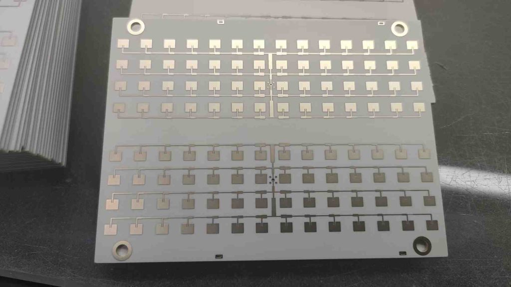
Radiofrequência (RF) PCBs são placas de circuito impresso especializadas projetadas para operar em altas frequências. Estas placas são cruciais em aplicações onde é necessário um tratamento preciso e eficiente de sinais de radiofrequência, como nas telecomunicações, redes sem fio, sistemas de radar, e outras aplicações de alta frequência. Os PCBs de RF são construídos com materiais e designs exclusivos para garantir perda mínima de sinal, alta integridade de sinal, e desempenho confiável em ambientes exigentes.
O que é um PCB de radiofrequência?
Uma RF PCB é um tipo de placa de circuito impresso projetada especificamente para lidar com sinais de alta frequência, normalmente na faixa de megahertz (MHz) para gigahertz (Ghz). Esses PCBs são utilizados em dispositivos e sistemas onde a transmissão e recepção de ondas de rádio são essenciais. O projeto e a construção de PCBs de RF exigem atenção meticulosa aos materiais, layout, e processos de fabricação para alcançar o desempenho elétrico e a confiabilidade desejados.
Projetar uma PCB RF envolve várias considerações críticas para garantir o desempenho ideal em altas frequências. As seções a seguir descrevem os principais aspectos do design de PCB de RF.
Os materiais usados em PCBs de RF desempenham um papel significativo em seu desempenho. Os materiais primários incluem:
Materiais de substrato: Substratos de alta frequência como Rogers, Ptfe (Teflon), e materiais cheios de cerâmica são comumente usados devido à sua baixa constante dielétrica (Dk) e baixo fator de dissipação (Df). Esses materiais ajudam a manter a integridade do sinal em altas frequências.
Folha de cobre: O cobre de alta pureza é usado para traços e planos condutores, fornecendo excelente condutividade elétrica e confiabilidade.
Pré-impregnado e laminado: Materiais pré-impregnados e laminados de alto desempenho são usados para unir as camadas, oferecendo baixa perda dielétrica e alta estabilidade térmica.
O empilhamento de camadas é um aspecto crucial do design de RF PCB:
Camadas de Sinal: Múltiplas camadas de sinal são usadas para rotear sinais de alta frequência. Essas camadas são projetadas com impedância controlada para garantir perda mínima de sinal e alta integridade de sinal.
Potência e planos terrestres: Energia dedicada e planos de aterramento fornecem referências de tensão estáveis e reduzem o ruído, o que é fundamental para manter a integridade do sinal em aplicações de RF.
Camadas de gerenciamento térmico: Vias térmicas e dissipadores de calor são incorporados para dissipar o calor gerado por componentes de alta frequência, garantindo um desempenho confiável.
Várias considerações importantes devem ser abordadas durante a fase de design:Integridade do Sinal: A alta integridade do sinal é mantida através de impedância controlada, roteamento de pares diferenciais, e minimizando os efeitos parasitários. O projeto deve garantir que os caminhos do sinal sejam tão curtos e diretos quanto possível.
Distribuição de energia: A distribuição eficiente de energia é garantida através de planos de energia dedicados, minimizando quedas de tensão e garantindo fornecimento de energia estável aos componentes de RF.
Gestão Térmica: Técnicas eficazes de gerenciamento térmico, como vias térmicas e espalhadores de calor, evitar o superaquecimento e garantir um desempenho consistente.
Estabilidade Mecânica: A placa deve fornecer suporte mecânico robusto para suportar as tensões de manuseio e operação em ambientes de alta frequência.
Confiabilidade: A confiabilidade a longo prazo é garantida através do uso de materiais de alta qualidade e processos de fabricação precisos, evitando problemas como delaminação e empenamento.
Quais materiais são usados em PCBs de RF?
Os materiais usados em PCBs de RF são selecionados por suas características elétricas, térmico, e propriedades mecânicas:
Substrato Rogers: Os materiais Rogers são amplamente utilizados em aplicações de RF devido à sua baixa constante dielétrica e baixa perda., que são essenciais para desempenho de alta frequência.
Ptfe (Teflon): PTFE é outra escolha popular para substratos de RF, oferecendo excelentes propriedades elétricas e baixa perda dielétrica.
Materiais Cheios de Cerâmica: Esses materiais fornecem alta estabilidade térmica e baixa perda dielétrica, tornando-os adequados para aplicações de RF de alta potência.
Folha de cobre: O cobre de alta pureza é usado para traços e planos condutores, fornecendo excelente condutividade elétrica e confiabilidade.
Pré-impregnado e laminado: Materiais pré-impregnados e laminados de alto desempenho são usados para unir as camadas, oferecendo baixa perda dielétrica e alta estabilidade térmica.
Qual é o tamanho dos PCBs de RF?
O tamanho dos PCBs de RF varia dependendo da aplicação e dos requisitos específicos de projeto:
Grossura: A espessura dos PCBs de RF pode variar de 0.5 mm a vários milímetros, dependendo do número de camadas e dos requisitos de gerenciamento térmico.
Dimensões: O comprimento e a largura dos PCBs são determinados pelo tamanho dos componentes e pelo layout do sistema. Eles podem variar de formatos pequenos para dispositivos compactos a placas grandes para sistemas de RF complexos.
O processo de fabricação de PCBs de RF
O processo de fabricação de PCBs de RF envolve várias etapas precisas e controladas para garantir alta qualidade e desempenho:
Materiais de substrato de alto desempenho, folhas de cobre, e materiais pré-impregnados são preparados e cortados em tamanhos apropriados para processamento.
As camadas são fabricadas laminando materiais condutores e isolantes em uma pilha. Cada camada é padronizada usando fotolitografia para definir o circuito.
Microvias e furos passantes são perfurados usando técnicas de perfuração mecânica ou a laser. Esses furos são então revestidos com cobre para criar conexões elétricas entre as camadas..
As camadas individuais são laminadas sob calor e pressão para formar um sólido, estrutura multicamadas. Este processo garante que todas as camadas estejam firmemente unidas e alinhadas.
Processos de fotolitografia e gravação são usados para criar circuitos de passo fino em cada camada, exigindo alta precisão para interconexões precisas.
Após a fabricação, a placa é montada com todos os componentes e conectores necessários. Testes rigorosos são realizados para garantir que a placa atenda a todas as especificações de projeto e requisitos de desempenho.
A área de aplicação de PCBs de RF
PCBs de RF são usados em uma ampla gama de aplicações de alta frequência:
Nas telecomunicações, PCBs de RF são usados em estações base, antenas, e outros equipamentos de comunicação de alta frequência para garantir transmissão e recepção confiáveis de sinal.
Em aplicações aeroespaciais e de defesa, PCBs de RF são usados em sistemas de radar, equipamento de comunicação, e sistemas de guerra eletrônica, onde o controle preciso dos sinais de RF é crítico.
Em dispositivos médicos, RF PCBs são usados em sistemas de imagem, equipamento de diagnóstico, e dispositivos de comunicação sem fio, onde o desempenho de alta frequência é essencial.
Em equipamentos de teste e medição, PCBs de RF são usados para suportar testes e análises de sinais de alta frequência, garantindo resultados precisos e confiáveis.
Quais são as vantagens dos PCBs RF?
Os PCBs de RF oferecem diversas vantagens que os tornam indispensáveis em aplicações de alta frequência:
Alto desempenho: Eles fornecem excelentes propriedades elétricas, permitindo transmissão confiável de sinal de alta frequência com perda mínima.
Integridade do Sinal: A alta integridade do sinal é mantida através de impedância controlada e materiais de baixa perda, garantindo transmissão de sinal precisa.
Gerenciamento térmico: Técnicas eficazes de gerenciamento térmico evitam o superaquecimento e garantem um desempenho consistente em altas frequências.
Estabilidade Mecânica: Propriedades mecânicas robustas garantem que a placa possa suportar as tensões de manuseio e operação em ambientes de alta frequência.
Confiabilidade: Materiais de alta qualidade e processos de fabricação precisos garantem confiabilidade e desempenho a longo prazo.
Perguntas frequentes
Quais são as principais considerações ao projetar um PCB RF?
As principais considerações incluem a seleção de materiais para desempenho elétrico e térmico, empilhamento de camadas para roteamento complexo, e garantindo a integridade do sinal, distribuição de energia, gerenciamento térmico, estabilidade mecânica, e confiabilidade.
Como os PCBs de RF diferem dos PCBs padrão?
Os PCBs de RF são projetados especificamente para aplicações de alta frequência, apresentando materiais e designs avançados para perda mínima de sinal, enquanto PCBs padrão são usados para aplicações eletrônicas gerais com requisitos de desempenho menos exigentes.
Qual é o processo de fabricação típico para PCBs de RF?
O processo envolve preparação de material, fabricação de camadas, perfuração e chapeamento, laminação, padronização de circuito, conjunto, e testes rigorosos para garantir alta qualidade e desempenho.
Quais são as principais aplicações dos PCBs de RF?
Esses PCBs são usados em telecomunicações, aeroespacial e defesa, dispositivos médicos, e equipamentos de teste e medição, fornecendo funcionalidade avançada e confiabilidade em aplicações de alta frequência.