CO., LTD")
IC ultrafino Substratos do pacote Fabricante.Somos um fabricante líder de substratos de pacotes IC ultrafinos, fornecendo soluções de ponta para dispositivos eletrônicos de alto desempenho. Nossas técnicas avançadas de fabricação garantem qualidade excepcional, permitindo miniaturização e funcionalidade aprimorada em diversas aplicações, de smartphones a dispositivos médicos. Confie em nós para soluções inovadoras, confiável, e substratos de pacote IC eficientes que atendem às demandas do mundo atual, orientado pela tecnologia.
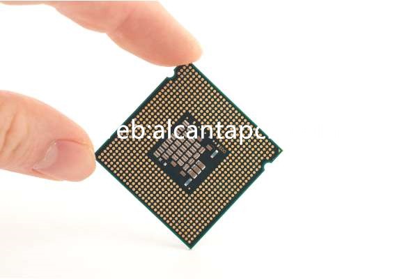
IC ultrafino (Circuito integrado) pacote substratos são um componente vital na eletrônica moderna, permitindo a miniaturização e melhor desempenho de vários dispositivos. Esses substratos são projetados para serem extremamente finos, mantendo ao mesmo tempo a energia elétrica necessária., térmico, e propriedades mecânicas para suportar CIs de alto desempenho. Substratos ultrafinos são particularmente importantes em aplicações onde o espaço é escasso, como smartphones, dispositivos vestíveis, e sistemas de computação avançados.
O que é um substrato de pacote IC ultrafino?
Um substrato de pacote IC ultrafino é um tipo especializado de placa de circuito impresso (PCB) projetado para fornecer uma plataforma para montagem e interconexão de ICs. Esses substratos são caracterizados por sua espessura mínima, normalmente menos de 100 micrômetros, que permite o desenvolvimento de embalagens eletrônicas ultracompactas. Apesar de sua magreza, substratos ultrafinos devem suportar interconexões de alta densidade, Gerenciamento térmico eficiente, e estabilidade mecânica robusta para garantir a operação confiável dos ICs que hospedam.
Guia de referência de design de substrato de pacote IC ultrafino
Projetar substratos de pacotes IC ultrafinos envolve uma abordagem abrangente para garantir desempenho e confiabilidade ideais.
A seleção de materiais é crítica para alcançar as propriedades desejadas em substratos ultrafinos:
Filmes de poliimida de alta densidade: Esses materiais oferecem excelente flexibilidade, alta estabilidade térmica, e bom isolamento elétrico, tornando-os ideais para aplicações ultrafinas.
Folhas de cobre: Usado para traços condutores e interconexões, as folhas de cobre devem ser finas, mas duráveis, para manter o desempenho elétrico sem adicionar volume significativo.
Adesivos e Dielétricos: Adesivos avançados e materiais dielétricos com baixas constantes dielétricas e alta condutividade térmica são usados para unir as camadas e fornecer isolamento.
A estrutura de camadas de substratos ultrafinos foi projetada para maximizar a eficiência e o desempenho do espaço:
Camadas de Sinal: Essas camadas são configuradas para minimizar a perda de sinal e diafonia. Técnicas como microstrip e stripline são usadas para manter a impedância controlada.
Camadas de energia e solo: Energia dedicada e planos de aterramento são cruciais para distribuição estável de energia e redução de ruído, garantindo operação confiável do IC.
Camadas de gerenciamento térmico: A integração de vias térmicas e espalhadores de calor ajuda a dissipar o calor de forma eficaz, evitando o superaquecimento de componentes críticos.
Camadas de interconexão: Interconexões de alta densidade (HDI) com microvias e furos passantes permitem roteamento complexo dentro do espaço restrito de substratos ultrafinos.
Quais materiais são usados em substratos de pacotes IC ultrafinos?
Os materiais usados em substratos de pacotes de IC ultrafinos são selecionados por sua capacidade de atender a rigorosos requisitos de desempenho:
Filmes de poliimida de alta densidade: Oferecendo excelente flexibilidade, Estabilidade térmica, e isolamento elétrico, esses filmes são uma escolha comum para aplicações ultrafinas.
Folhas de cobre: Folhas de cobre finas, porém duráveis, são usadas para traços condutores e interconexões, garantindo desempenho elétrico confiável.
Adesivos e Dielétricos: Adesivos avançados e materiais dielétricos com baixas constantes dielétricas e alta condutividade térmica são usados para unir as camadas e fornecer isolamento.
Resinas Epóxi Reforçadas: Esses materiais aumentam a resistência mecânica do substrato, mantendo um perfil baixo.
Qual é o tamanho dos substratos de pacote IC ultrafinos?
O tamanho dos substratos ultrafinos do pacote IC varia dependendo da aplicação específica e dos requisitos do dispositivo:
Grossura: Substratos ultrafinos são normalmente menores que 100 micrômetros de espessura, com alguns designs atingindo espessuras ainda mais baixas para acomodar os menores formatos.
Comprimento e largura: Essas dimensões são determinadas pelo tamanho do IC e pelo layout das interconexões. Os tamanhos típicos variam de alguns milímetros para CIs pequenos a vários centímetros para pacotes maiores.
O processo de fabricação de substratos de pacotes IC ultrafinos
O processo de fabricação de substratos de embalagens IC ultrafinos envolve várias etapas precisas e controladas para garantir alta qualidade e desempenho:
Filmes de poliimida de alta densidade, materiais condutores, e adesivos são preparados e cortados em tamanhos apropriados para processamento.
As camadas são fabricadas laminando materiais condutores e isolantes em uma pilha. Cada camada é padronizada usando fotolitografia para definir o circuito.
Microvias e furos passantes são perfurados usando técnicas de perfuração mecânica ou a laser. Esses furos são então revestidos com cobre para criar conexões elétricas entre as camadas..
Processos de fotolitografia e gravação são usados para criar circuitos de passo fino em cada camada. Esta etapa requer alta precisão para garantir interconexões precisas e confiáveis.
Após a fabricação da camada, as camadas são laminadas juntas sob calor e pressão. O substrato montado passa por testes rigorosos, incluindo testes elétricos, ciclagem térmica, e testes de estresse mecânico, para garantir desempenho e confiabilidade.
A área de aplicação de substratos de pacotes IC ultrafinos
Substratos de pacote IC ultrafinos permitem recursos avançados em uma ampla gama de aplicações:
Em smartphones, comprimidos, e dispositivos vestíveis, substratos ultrafinos suportam a integração compacta e eficiente de CIs avançados, melhorando o desempenho e a funcionalidade enquanto reduz o tamanho e o peso.
Em servidores, data centers, e supercomputadores, substratos ultrafinos permitem a integração de processadores e módulos de memória poderosos em um formato compacto, facilitando o processamento e armazenamento rápido de dados.
Esses substratos são essenciais na infraestrutura de telecomunicações, incluindo estações base e equipamentos de rede, fornecendo conectividade confiável e de alta velocidade em um espaço compacto.
Em vários produtos eletrônicos de consumo, de dispositivos domésticos inteligentes a consoles de jogos, substratos ultrafinos permitem alto desempenho em ambientes elegantes, projetos com eficiência de espaço.
Em imagens médicas e equipamentos de diagnóstico, substratos ultrafinos suportam aquisição e processamento de dados em alta velocidade, melhorando a precisão e eficiência em procedimentos médicos.
Quais são as vantagens dos substratos de pacote IC ultrafinos?
Substratos de pacotes IC ultrafinos oferecem diversas vantagens que os tornam indispensáveis para aplicações eletrônicas avançadas:
Design Compacto: O perfil ultrafino permite a miniaturização de embalagens eletrônicas, permitindo dispositivos mais compactos e portáteis.
Alto desempenho: Materiais e design otimizados garantem alta integridade de sinal, baixa perda de energia, e gerenciamento térmico eficaz.
Confiabilidade aprimorada: Processos e materiais de fabricação avançados proporcionam alta confiabilidade, garantindo desempenho de longo prazo em ambientes exigentes.
Flexibilidade: A natureza fina e flexível desses substratos os torna adequados para uma ampla gama de aplicações, desde dispositivos rígidos de alto desempenho até eletrônicos flexíveis e vestíveis.
Escalabilidade: Substratos ultrafinos podem ser personalizados para atender às necessidades específicas de diversas aplicações, desde pequenos dispositivos de consumo até grandes sistemas industriais.
Perguntas frequentes
Quais são as principais considerações no projeto de substratos de pacotes de IC ultrafinos?
As principais considerações incluem a seleção de materiais para propriedades elétricas e térmicas, otimização da estrutura da camada para integridade do sinal e gerenciamento térmico, e garantindo estabilidade mecânica e confiabilidade.
Como os substratos de pacotes IC ultrafinos diferem dos PCBs padrão?
Substratos de pacotes IC ultrafinos são significativamente mais finos, com mais camadas e maior densidade de interconexão, projetado para lidar com frequências e níveis de potência mais altos em comparação com PCBs padrão, tornando-os adequados para aplicações avançadas.
Qual é o processo de fabricação típico para substratos de embalagens IC ultrafinos?
O processo envolve preparação de material, fabricação de camadas, perfuração e chapeamento, padronização de circuito, conjunto, e testes rigorosos para garantir alto desempenho e confiabilidade.
Quais são as principais aplicações de substratos de embalagens IC ultrafinos?
Esses substratos são usados em dispositivos móveis, computação de alto desempenho, Telecomunicações, eletrônica de consumo, e dispositivos médicos, fornecendo funcionalidade avançada e confiabilidade nesses campos.