CO.,LTD")
Hersteller von HF-Modulsubstraten. Hochfrequenz und Hohe Geschwindigkeit Material Verpackungssubstrat Produktion. Wir bieten fortschrittliche Microtrace-RF-Verpackungssubstrate von an 2 Schicht zu 30 Lagen.
In modernen elektronischen Geräten, Die Rolle von HF-Modulen ist immer wichtiger geworden. Von Smartphones bis hin zu Internet-of-Things-Geräten, Sie alle setzen auf leistungsstarke Hochfrequenztechnologie. Jedoch, Hinter der Stabilität und Leistung dieser HF-Module steckt eine Kombination aus anspruchsvollen Design- und Herstellungsprozessen. In diesem Prozess, Hersteller von HF-Modulsubstraten spielen eine Schlüsselrolle, und ihre Technologie und Innovation treiben die gesamte Branche voran.
Was ist ein HF-Modulsubstrat??
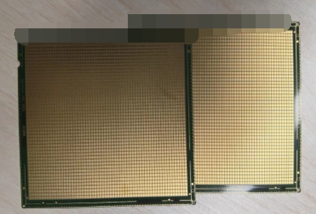
HF-Modulsubstrat, als PCB bezeichnet (Leiterplatte), ist eine Leiterplatte, die speziell für den Einsatz im Hochfrequenzbereich entwickelt wurde (Funkfrequenz, Rf) elektronische Geräte. In der modernen Kommunikations- und Funktechnologie, Eine entscheidende Rolle spielen HF-Modulsubstrate. Sie sind nicht nur Träger zur Verbindung und Unterstützung von Hochfrequenz-Schaltungskomponenten, sondern auch eine Schlüsselkomponente, um den stabilen Betrieb drahtloser Kommunikationsgeräte sicherzustellen.
Das Design und die Herstellung von HF-Modulsubstraten sind komplexer und präziser als bei herkömmlichen Leiterplatten. Dies liegt daran, dass Hochfrequenzschaltungen in einem Hochfrequenzbereich arbeiten und extrem hohe Anforderungen an die Signalintegrität stellen, Übertragungsverlust und elektromagnetische Störungen. daher, Bei der Gestaltung des HF-Modulsubstrats müssen viele Faktoren berücksichtigt werden, inklusive Optimierung von Layout und Verkabelung, Design von Signalübertragungsleitungen, Effizienz der Kraftübertragung, und der Schutz von EMI (Elektromagnetische Störung, elektromagnetische Störungen) und EMV (Elektromagnetische Verträglichkeit, elektromagnetische Verträglichkeit). verwalten.
Auf dem HF-Modulsubstrat, verschiedene Hochfrequenzkomponenten wie Antennen, Verstärker, Filter, Modems, usw. sind präzise angeordnet und verbunden. Die Position und Anordnung dieser Komponenten ist für die Übertragung und den Empfang von HF-Signalen von entscheidender Bedeutung. Gleichzeitig, Die Auswahl des PCB-Materials beeinflusst auch die Leistung von HF-Schaltkreisen. Zu den gängigen Substratmaterialien für HF-Module gehört FR-4, PTFE (Polytetrafluorethylen), Rogers, Arlon, usw. Sie haben unterschiedliche Dielektrizitätskonstanten, thermische Eigenschaften und Verlustfaktoren und können entsprechend den spezifischen Anwendungsanforderungen ausgewählt werden.
Im Allgemeinen, HF-Modulsubstrate spielen in der modernen drahtlosen Kommunikationstechnologie eine unersetzliche Rolle. Sie bieten zuverlässige Stützstrukturen und optimierte Signalübertragungsumgebungen für verschiedene elektronische Hochfrequenzgeräte, Förderung der Entwicklung und des Fortschritts der Kommunikationstechnologie. daher, Kontinuierliche Verbesserung und Innovation im Design, Die Herstellung und Anwendung von HF-Modulsubstraten ist eines der wichtigen Themen in der heutigen Elektronikindustrie.
Referenzhandbuch für das Substratdesign von HF-Modulen.
Das Entwerfen von HF-Modulsubstraten erfordert hochentwickelte Technologie und Fachwissen. Im Design-Guide, Das Verständnis von HF-Signalen ist ein entscheidender Teil. Die Eigenschaften von HF-Signalen unterscheiden sich stark von Gleichstromkreisen oder Niederfrequenzsignalen, Daher erfordern sie eine eingehende Analyse und ein umfassendes Verständnis. Designer müssen die Häufigkeit berücksichtigen, Baudrate, Leistung und andere Parameter des Signals, und entsprechende Maßnahmen ergreifen, um die Genauigkeit und Stabilität der Signalübertragung und des Signalempfangs sicherzustellen.
Ein weiterer wichtiger Aspekt sind Layout- und Routing-Spezifikationen. Eine gute Anordnung und Verkabelung kann Signalinterferenzen und Übersprechen minimieren und die Systemleistung und -stabilität verbessern. Während des Designprozesses, Der Standort und die Verkabelungswege von HF-Komponenten müssen angemessen angeordnet sein, um Störungen zwischen HF-Signalen und anderen Signalen oder Stromleitungen zu vermeiden.
Zusätzlich, Signalintegrität ist ein weiterer wichtiger Aspekt in den Designrichtlinien. Die Übertragung von HF-Signalen wird durch die Signalintegrität beeinflusst, Daher müssen Maßnahmen ergriffen werden, um die Signalintegrität sicherzustellen, B. die Verwendung eines geeigneten Erdungskabeldesigns, Differenzielle Signalführung, und Impedanzanpassung.
Endlich, der Umgang mit elektromagnetischen Störungen (EMI) und elektromagnetische Verträglichkeit (EMV) ist ebenfalls Teil der Gestaltungsrichtlinien, die nicht außer Acht gelassen werden dürfen. Hochfrequenzschaltungen erzeugen oft starke elektromagnetische Strahlung, Dies kann zu Störungen bei umliegenden elektronischen Geräten und Systemen führen. daher, Designer müssen Maßnahmen ergreifen, um elektromagnetische Strahlung zu reduzieren und sicherzustellen, dass Produkte den relevanten Normen zur elektromagnetischen Verträglichkeit entsprechen.
Um zusammenzufassen, Das Entwerfen eines HF-Modulsubstrats erfordert eine umfassende Berücksichtigung mehrerer Faktoren, einschließlich des Verständnisses von HF-Signalen, Layout- und Verkabelungsspezifikationen, Signalintegrität, und EMI/EMV-Management. Hersteller stellen oft detaillierte Designrichtlinien zur Verfügung, um Designern dabei zu helfen, während des Designprozesses verschiedene Faktoren zu berücksichtigen, um die Leistung und Zuverlässigkeit des Endprodukts sicherzustellen.
Welches Material wird im HF-Modulsubstrat verwendet??
Die Materialauswahl des HF-Modulsubstrats ist entscheidend, da sie sich direkt auf die Leistung und Stabilität des Endprodukts auswirkt. Zu den gängigen Substratmaterialien für HF-Module gehört FR-4, PTFE (Polytetrafluorethylen), Rogers und Arlon, usw. Jedes Material hat einzigartige Eigenschaften, die je nach spezifischen Anwendungsanforderungen abgewogen werden müssen.
FR-4 ist eines der am häufigsten verwendeten Substratmaterialien und weist eine gute mechanische Festigkeit und Hitzebeständigkeit auf. Die Dielektrizitätskonstante und der Verlustfaktor sind moderat, Dadurch eignet es sich für allgemeine HF-Anwendungen. Jedoch, für hohe Frequenzen oder Anwendungen mit höheren Anforderungen an die Signalintegrität, Möglicherweise ist eine bessere Leistung erforderlich.
PTFE (Polytetrafluorethylen) ist ein Material mit geringen Verlusten und einer hohen Dielektrizitätskonstante, Machen Sie es hervorragend in hochfrequenten Anwendungen. Es verfügt außerdem über gute thermische Eigenschaften und eignet sich für Anwendungen, die in Umgebungen mit hohen Temperaturen über einen langen Zeitraum stabil arbeiten, wie Radarsysteme oder Satellitenkommunikationsgeräte.
Spezialmaterialien wie Rogers und Arlon sind für Hochleistungs-HF-Anwendungen konzipiert. Sie verfügen über hervorragende dielektrische Eigenschaften und Stabilität und eignen sich für Szenarien mit äußerst anspruchsvoller Signalübertragung und -empfang, wie Basisstationen für die drahtlose Kommunikation oder Hochgeschwindigkeits-Datenübertragungsgeräte.
Bei der Auswahl der Substratmaterialien für HF-Module, Faktoren wie die Dielektrizitätskonstante, Verlustfaktor, thermische Eigenschaften, und Kosten müssen umfassend berücksichtigt werden. Unterschiedliche Materialien eignen sich für unterschiedliche Szenarien und müssen entsprechend den spezifischen Anwendungsanforderungen genau ausgewählt werden. Gleichzeitig, Hersteller bieten in der Regel entsprechende technische Unterstützung und Beratung an, um Kunden bei der Auswahl des besten Materials zu unterstützen.
Welche Größe haben HF-Modulsubstrate??
Die Größe des HF-Modulsubstrats ist ein entscheidender Designaspekt für verschiedene Anwendungsanforderungen. Von winzigen Geräten bis hin zu großen Basisstationen, HF-Modulsubstrate unterschiedlicher Größe haben einzigartige Verwendungszwecke und Designanforderungen.
Für Miniaturgeräte, wie Smartphones, tragbare Geräte, oder medizinische Gesundheitsmonitore, Die Größe muss oft minimiert werden. Da der physische Platz dieser Geräte sehr begrenzt ist, Das HF-Modulsubstrat muss klein genug sein, um in das Gesamtdesign des Geräts zu passen. daher, Die Größe des für ein Miniaturgerät erforderlichen HF-Modulsubstrats kann nur wenige Millimeter betragen. Diese Anforderung an die geringe Größe stellt in der Regel größere Herausforderungen an das PCB-Design und -Layout, anspruchsvolle Techniken und innovative Lösungen von Konstrukteuren erfordern.
Im Gegensatz, Die Größe des HF-Modulsubstrats, das für große Basisstationsgeräte erforderlich ist, kann relativ groß sein. Basisstationsgeräte müssen häufig große Mengen an Datenverkehr und komplexe Kommunikationsaufgaben bewältigen, Daher muss das Substrat des HF-Moduls über mehr Verarbeitungsfähigkeiten und Schnittstellen verfügen. Dies führt zu relativ großen Abmessungen der Basisstationsausrüstung, und auch das HF-Modulsubstrat muss entsprechend dimensioniert sein, um seinen Leistungs- und Funktionsanforderungen gerecht zu werden. In diesem Fall, Die Vergrößerung bringt möglicherweise mehr Überlegungen zur thermischen und mechanischen Stabilität mit sich, Gleichzeitig steigen auch die Kosten für das Gesamtgerät.
Zusätzlich zur Größe des Geräts, Die Größenauswahl wird von anderen Faktoren beeinflusst, inklusive Leistung, Stromverbrauch, kosten, und physischer Raum. Zum Beispiel, Für einige Anwendungen gelten möglicherweise äußerst strenge Anforderungen an den Stromverbrauch, Daher muss das HF-Modulsubstrat kleiner und effizienter gestaltet werden. Bei anderen Anwendungen geht es möglicherweise mehr um Kosten und Platzbedarf, und kann im Austausch für ein günstigeres oder kompakteres Design etwas an Leistung einbüßen.
Gesamt, Die Auswahl der Substratgröße eines HF-Moduls ist ein komplexer Kompromissprozess, der eine umfassende Berücksichtigung mehrerer Faktoren erfordert. Ob es sich um ein Mikrogerät oder eine große Basisstation handelt, Es muss entsprechend den spezifischen Anwendungsanforderungen angepasst werden, um sicherzustellen, dass das HF-Modulsubstrat die beste Leistungsbalance erreichen kann, Stromverbrauch, Kosten und physischer Raum.
Der Herstellungsprozess von HF-Modulsubstraten.
Der Herstellungsprozess von HF-Modulsubstraten ist ein komplexes und präzises Projekt, Dies beinhaltet Präzisionsoperationen und Qualitätskontrolle in mehreren Verbindungen. Im Folgenden finden Sie eine detaillierte Einführung in jeden Aspekt des Herstellungsprozesses für HF-Modulsubstrate:
Der erste Schritt im Herstellungsprozess ist die Designüberprüfung. In diesem Stadium, Ingenieure verwenden professionelle Designsoftware, um Designzeichnungen des HF-Modulsubstrats basierend auf den Bedürfnissen und Spezifikationen des Kunden zu erstellen. Die Designverifizierung gewährleistet die Genauigkeit und Machbarkeit des Designs, um die Leistungs- und Funktionsanforderungen des Produkts zu erfüllen.
Sobald die Designüberprüfung abgeschlossen ist, Im nächsten Schritt geht es um die Beschaffung der benötigten Rohstoffe. Zu diesen Rohstoffen zählen Substratmaterialien, Schaltungskomponenten, Chemikalien, usw. Hersteller arbeiten mit Lieferanten zusammen, um sicherzustellen, dass die eingekauften Rohstoffe den Qualitätsstandards und Produktanforderungen entsprechen.
Nachdem die Rohstoffe vorbereitet sind, Der nächste Schritt besteht darin, das Design auf das Substrat zu drucken. Dies wird typischerweise durch eine Leiterplatte erreicht (Leiterplatte) Fertigungsausrüstung, Dazu gehören fortschrittliche Fotolithographie- und Ätztechnologien. Die Präzision des Druckprozesses ist entscheidend für die Gewährleistung der Genauigkeit und Leistung der Schaltung.
Nachdem der Druckvorgang abgeschlossen ist, Das Substrat muss einer Reihe chemischer Behandlungen unterzogen werden. Zu diesen Prozessen gehört die Reinigung, Entfernen restlicher Druckfarbe, und das Hinzufügen chemischer Beschichtungen. Chemische Behandlungen sorgen für Glätte und Sauberkeit der Substratoberfläche für nachfolgende Prozessschritte.
Als nächstes werden Löcher in die Grundplatte gebohrt, um Schaltkreiskomponenten und Anschlüsse zu montieren. Dieser Schritt wird üblicherweise mit einer CNC-Bohrmaschine durchgeführt, und die Position und Größe der Löcher müssen genau mit der Konstruktionszeichnung übereinstimmen, um die Konnektivität und Zuverlässigkeit der Schaltung sicherzustellen.
Nachdem das Bohren abgeschlossen ist, Der Untergrund muss metallisiert werden. Dabei wird das Loch mit einer leitenden Metallschicht beschichtet, normalerweise Kupfer. Die Metallisierung gewährleistet die Zuverlässigkeit der Verbindung und die Leitfähigkeit des Stromkreises, Dadurch werden die Produktleistung und -stabilität verbessert.
Sobald die Metallisierung abgeschlossen ist, Der nächste Schritt besteht darin, die Schaltungskomponenten und Anschlüsse auf dem Substrat zu montieren. Dazu gehören Prozessschritte wie das Löten, Patchen, und Plug-Ins. Der Montageprozess erfordert ein hohes Maß an Geschick und Präzision, um eine korrekte Installation und Verbindung der Komponenten sicherzustellen.
Der letzte Schritt besteht darin, das fertige Produkt zu testen. Das Testen umfasst Funktionstests, Leistungstests und Zuverlässigkeitstests. Erst nach bestandener strenger Prüfung darf das Produkt das Werk verlassen und in Betrieb genommen werden.
Um zusammenzufassen, Der Herstellungsprozess von HF-Modulsubstraten umfasst mehrere wichtige Verbindungen, Jedes davon erfordert ein hohes Maß an Präzision und Qualitätskontrolle. Nur durch strenge Herstellungsprozesse und Qualitätsmanagement können wir HF-Modulsubstratprodukte mit hervorragender Leistung herstellen, Stabilität und Zuverlässigkeit.
Der Anwendungsbereich von HF-Modulsubstraten.
Als Schlüsselkomponente der Hochfrequenztechnologie, Das Substrat von HF-Modulen spielt in verschiedenen Bereichen eine wichtige Rolle, leistet wichtige Unterstützung für technologische Innovationen, und fördert die Entwicklung und den Fortschritt der Branche. Im Folgenden sind die Anwendungen von HF-Modulsubstraten in verschiedenen Bereichen aufgeführt:
Kommunikationsfeld
Im Bereich Kommunikation, HF-Modulsubstrate werden häufig in drahtlosen Kommunikationsgeräten verwendet, wie Basisstationen, Mobiltelefone, Modems, usw. Sie realisieren drahtlose Kommunikationsverbindungen durch das Senden und Empfangen von Hochfrequenzsignalen, Bereitstellung effizienter und bequemer Kommunikationsmethoden für Menschen.
Medizinischer Bereich
Im medizinischen Bereich, HF-Modulsubstrate werden in medizinischen Geräten verwendet, wie MRT (Magnetresonanztomographie), Herzschrittmacher, drahtlose Überwachungsgeräte, usw. Sie können drahtlose Datenübertragung und Fernüberwachung realisieren, Bereitstellung intelligenterer und praktischerer Lösungen für die medizinische Industrie.
Militärischer Bereich
Im militärischen Bereich, HF-Modulsubstrate werden häufig in militärischen Geräten wie Radarsystemen verwendet, Kommunikationsausrüstung, und Navigationssysteme. Sie verfügen über ein hohes Maß an Entstörfähigkeit und Stabilität, und kann in rauen Umgebungen zuverlässig arbeiten, Bereitstellung starker Unterstützung für die nationale Verteidigungssicherheit.
Luft- und Raumfahrtbereich
Im Luft- und Raumfahrtbereich, HF-Modulsubstrate werden in der Flugzeugkommunikation eingesetzt, Navigation, Radar, Telemetrie und andere Systeme. Sie haben den Vorteil, dass sie leicht sind, hohe Leistung und Zuverlässigkeit, und kann die strengen Anforderungen an leistungsstarke elektronische Geräte im Luft- und Raumfahrtbereich erfüllen.
Automobilbereich
Im Automotive-Bereich, HF-Modulsubstrate werden häufig in der Fahrzeugkommunikation eingesetzt, Fahrzeugunterhaltung, Fahrzeugnavigation, Intelligente Fahrassistenzsysteme, usw. Sie ermöglichen die drahtlose Kommunikation innerhalb und zwischen Fahrzeugen, Verbesserung der Sicherheit, Komfort und Intelligenz von Fahrzeugen.
Industrieller Kontrollbereich
Im Bereich der industriellen Steuerung, HF-Modulsubstrate werden in industriellen Automatisierungsgeräten verwendet, Sensornetzwerke, Fernüberwachungssysteme, usw. Sie ermöglichen die Datenübertragung und Kommunikation zwischen Geräten, Verbesserung der Effizienz und des Automatisierungsgrades der industriellen Produktion.
Um zusammenzufassen, HF-Modulsubstrate spielen in verschiedenen Bereichen wie der Kommunikation eine wichtige Rolle, medizinisch, Militär, Luft- und Raumfahrt, Automobil- und Industriesteuerung, Bereitstellung wichtiger Unterstützung für Innovationen in verschiedenen Branchen und Förderung der Entwicklung und des Fortschritts von Wissenschaft und Technologie.
Was sind die Vorteile von RF-Modulsubstraten??
Die Vorteile von HF-Modulsubstraten spielen in heutigen drahtlosen Kommunikationssystemen eine entscheidende Rolle. Im Vergleich zur herkömmlichen Leitungsverkabelung, HF-Modulsubstrate weisen eine Reihe bedeutender Vorteile auf, die sie zu einem unverzichtbaren Bestandteil drahtloser Kommunikationssysteme machen.
Erste, Das HF-Modulsubstrat weist einen höheren Integrationsgrad auf. Durch die Integration von HF-Geräten und Komponenten auf der Leiterplatte, Das HF-Modulsubstrat kann die Größe und das Gewicht des Systems erheblich reduzieren. Dieser Integrationsgrad verbessert nicht nur die Gesamtleistung des Systems, sondern reduziert auch die Komplexität und Kosten des Systems.
Zweitens, Das HF-Modulsubstrat weist eine bessere Signalintegrität auf. Als hochwertiges Medium, PCB kann eine gute Signalübertragungsumgebung bieten und Signaldämpfung und -verzerrung wirksam reduzieren. Dies bedeutet, dass das HF-Modulsubstrat eine Signalübertragung über größere Entfernungen erreichen und eine gute Kommunikationsqualität in komplexen elektromagnetischen Umgebungen aufrechterhalten kann.
Zusätzlich, Das HF-Modulsubstrat weist einen geringeren Signalverlust auf. Im Vergleich zur herkömmlichen Leitungsverkabelung, PCB kann Signalübertragungsverluste durch optimiertes Layout und Design reduzieren. Dadurch kann das System eine höhere Effizienz und einen geringeren Energieverbrauch erreichen, Dadurch wird die Lebensdauer der Geräte verlängert und die Betriebskosten gesenkt.
Endlich, Das HF-Modulsubstrat ist kleiner. Aufgrund der kontinuierlichen Weiterentwicklung der PCB-Technologie, Jetzt können kleinere Leiterplattendesigns realisiert werden, wodurch das gesamte System kompakter und tragbarer wird. Dies ist besonders wichtig für einige Anwendungen, die strenge Platzanforderungen haben, wie Smartphones, tragbare Geräte, und IoT -Sensoren.
Zusammenfassend, HF-Modulsubstrat, als Schlüsselkomponente drahtloser Kommunikationssysteme, hat viele Vorteile wie eine höhere Integration, bessere Signalintegrität, geringerer Signalverlust, und kleinere Größe. Diese Vorteile verbessern nicht nur die Leistung und Zuverlässigkeit des Systems, sondern fördern auch die kontinuierliche Entwicklung und Innovation der drahtlosen Kommunikationstechnologie. daher, Hersteller von HF-Modulsubstraten spielen in der modernen Elektronikindustrie eine unersetzliche Rolle, Bereitstellung starker Unterstützung für Innovationen in verschiedenen Anwendungsbereichen.
FAQ
Wie lang ist der Herstellungszyklus des HF-Modulsubstrats??
Der Herstellungszyklus von HF-Modulsubstraten hängt normalerweise von der spezifischen Projektgröße und -komplexität ab, sowie die Produktionskapazitäten und den Prozessablauf des Herstellers. Allgemein gesprochen, Ein einfaches HF-Modulsubstrat kann in wenigen Tagen hergestellt werden, während komplexe Projekte Wochen oder sogar länger dauern können. Vor der Herstellung, Faktoren wie Designverifizierung, Rohstoffbeschaffung, und die Produktionsplanung wirken sich alle auf die Länge des Herstellungszyklus aus.
Was kostet das HF-Modulsubstrat??
Die Kosten von HF-Modulsubstraten werden von vielen Faktoren beeinflusst, einschließlich der Art des ausgewählten Materials, Brettdicke, Anzahl der Schichten, Größe, Oberflächenbehandlung, Komplexität und Bestellmenge. Allgemein gesprochen, HF-Modulsubstrate mit Hochleistungsmaterialien und komplexen Designs werden mehr kosten. Hersteller basieren ihre Angebote in der Regel auf den spezifischen Anforderungen des Kunden, unter Berücksichtigung verschiedener Faktoren, um die endgültigen Kosten zu ermitteln.
Welche besonderen Fähigkeiten sind für das Design von HF-Modulsubstraten erforderlich??
Das Entwerfen von HF-Modulsubstraten erfordert ein tiefgreifendes Verständnis der HF-Schaltkreise und des PCB-Layouts, sowie die Fähigkeit, professionelle Designsoftware für das Layout gekonnt einzusetzen, Verdrahtung, und Simulation. Designer müssen die Eigenschaften von Hochfrequenzsignalen verstehen und die Layout- und Verbindungsspezifikationen von Hochfrequenzschaltungen beherrschen, um die Leistung und Stabilität des HF-Modulsubstrats sicherzustellen. Zusätzlich, für komplexe Projekte, Möglicherweise sind auch Fachkenntnisse wie Signalintegritätsanalyse und EMI/EMV-Design erforderlich.
So stellen Sie die Zuverlässigkeit des HF-Modulsubstrats sicher?
Die Gewährleistung der Zuverlässigkeit von HF-Modulsubstraten ist eine der wichtigen Aufgaben der Hersteller. Sie wenden strenge Qualitätskontrollprozesse an, inklusive Rohstoffinspektion, Überwachung des Produktionsprozesses, Inspektion und Prüfung des fertigen Produkts, um sicherzustellen, dass jedes Substrat den Designanforderungen und Kundenerwartungen entspricht. Zusätzlich, Hersteller werden auch Zuverlässigkeitstests an Produkten durchführen, wie Thermoschocktests, Wärme- und Feuchtigkeitszyklustests, usw., um ihre Stabilität und Zuverlässigkeit unter verschiedenen Umgebungsbedingungen zu überprüfen.