CO.,LTD")
Halbleiter BGA-Substrats Hersteller, Wir produzieren hauptsächlich ein ultra-kleines Bump-Tonhöhe-Substrat, Ultra-kleiner Spur und Abstand Verpackungssubstrat
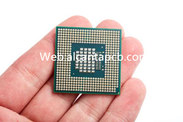
Halbleiter-BGA (Kugelgitter-Array) Substrat ist eine hochdichte Verpackungstechnologie, die häufig bei der Verpackung und Verbindung integrierter Schaltkreise eingesetzt wird (ICs). Als Verbindungsmedium werden kugelförmige Lotkugeln verwendet, sodass die Chips auf der Platine über diese kugelförmigen Lötkugeln mit der Hauptplatine oder anderen Geräten verbunden werden können. Im Vergleich zu herkömmlichen Pin-basierten Verpackungen, Mit BGA-Substraten können eine höhere Verbindungsdichte und eine bessere elektrische Leistung erreicht werden.
BGA-Substrate bestehen üblicherweise aus Halbleitermaterialien, wie z.B. Silizium, Galliumarsenid (GaAs), usw. Seine Struktur besteht aus Chips, Verpackungssubstrate, kugelförmige Lötkugeln und Anschlüsse. Während des Herstellungsprozesses, Chips werden auf einem Substrat verpackt und durch Löttechniken verbunden. Diese Verpackungstechnologie ermöglicht BGA-Substraten eine höhere Zuverlässigkeit und bessere Wärmemanagementfähigkeiten, Dadurch eignen sie sich für eine Vielzahl leistungsstarker elektronischer Geräteanwendungen.
Zu den Hauptmerkmalen des BGA-Substrats gehören::
Verbindung mit hoher Dichte: Durch kugelförmige Lötkugel-Verbindungstechnik, Das BGA-Substrat kann Verbindungen mit höherer Dichte erreichen, Dadurch können mehr Chips und Geräte auf der Leiterplatte untergebracht werden.
Hervorragende elektrische Leistung: BGA-Substrat hat einen kürzeren Signalübertragungsweg und einen kleineren Widerstand und eine geringere Induktivität, Dadurch wird die Leistung und Stabilität der Schaltung verbessert.
Gutes Thermomanagement: Aufgrund des guten Kontakts zwischen den Lotkugeln und dem Substrat, Das BGA-Substrat kann die vom Chip erzeugte Wärme effektiver übertragen und verteilen, Reduzierung der thermischen Belastung des Chips und Verbesserung der Zuverlässigkeit des Systems.
Im Allgemeinen, Halbleiter-BGA-Substrat ist eine fortschrittliche Verpackungstechnologie, die stabile und leistungsstarke Lösungen für die Entwicklung und Herstellung elektronischer Geräte bietet. Mit der kontinuierlichen Entwicklung und dem Fortschritt der Elektronikindustrie, BGA-Substrate werden weiterhin eine wichtige Rolle spielen, Förderung der kontinuierlichen Innovation der Technologie und der Erweiterung der Anwendungen.
Was ist der Herstellungsprozess von Halbleiter-BGA-Substraten??
Der Herstellungsprozess von Halbleiter-BGA-Substraten umfasst mehrere wichtige Schritte, Jeder Schritt ist entscheidend und beeinflusst die Qualität und Leistung des Endprodukts. Diese wichtigen Schritte werden im Folgenden detailliert beschrieben:
Design: Der erste Schritt bei der Herstellung eines Halbleiter-BGA-Substrats ist das Design. In diesem Stadium, Der Hersteller arbeitet mit dem Kunden zusammen, um die Spezifikationen festzulegen, Maße, und Layout des Untergrundes. Das Designteam verwendet CAD-Software, um zu entwerfen und sicherzustellen, dass die Verkabelung und das Steckerlayout des Substrats den Produktanforderungen entsprechen.
Materialauswahl: Die Auswahl leistungsstarker Halbleitermaterialien, die für eine bestimmte Anwendung geeignet sind, ist ein entscheidender Schritt im Herstellungsprozess. Zu diesen Materialien gehören Substratmaterialien, Verpackungsmaterialien, Metalldrähte, usw. Hersteller wählen geeignete Materialien basierend auf Produktanforderungen und Leistungsindikatoren aus, um die Stabilität und Zuverlässigkeit des Substrats sicherzustellen.
Grafik- und Bildbearbeitung: Der Hersteller importiert das entworfene BGA-Substratbild in die Grafik- und Bildverarbeitungssoftware, und führen Sie verschiedene Parameteranpassungen und Optimierungen durch, um sicherzustellen, dass das endgültige Bild die Designanforderungen genau widerspiegelt.
Photolithographie: Während des Herstellungsprozesses, Mithilfe der Photolithographie werden entworfene Muster auf die Substratoberfläche übertragen. Bei der Fotolithographie handelt es sich um einen präzisen Prozess, bei dem lichtempfindliches Harz und Fotolack verwendet werden, um Muster auf die Oberfläche eines Substrats zu projizieren und entsprechende chemische Behandlungen durchzuführen, um das gewünschte Muster zu bilden.
Radierung: Nach der Fotolithographie, Um unerwünschte Teile des Materials von der Substratoberfläche zu entfernen, ist ein Ätzprozess erforderlich, Hinterlassen der gewünschten Muster und Anschlüsse. Beim Ätzen können Methoden wie chemisches Ätzen oder physikalisches Ätzen zum Einsatz kommen, und der geeignete Ätzprozess kann je nach Material und Designanforderungen ausgewählt werden.
Metallisation: Nachdem das Ätzen abgeschlossen ist, Die Oberfläche des Substrats muss metallisiert werden, um die Leitfähigkeit des Steckverbinders zu verbessern. Bei der Metallisierung können Methoden wie Elektroplattieren oder chemische Gasphasenabscheidung zum Einsatz kommen, um eine Metallschicht auf der Oberfläche eines Substrats abzuscheiden und so einen leitfähigen Verbinder zu bilden.
Verpackung: Unter Packaging versteht man den Prozess der Montage eines integrierten Schaltkreischips auf einem BGA-Substrat. Hersteller verwenden hochentwickelte Geräte, um die Chips mit dem Substrat zu verbinden und sie durch Löten oder andere Befestigungsmethoden an Ort und Stelle zu halten. Der Verpackungsprozess umfasst auch Schritte wie die Installation eines Kühlkörpers und das Einfüllen des Verpackungsklebers, um die Stabilität und Wärmeableitungsleistung des Chips zu verbessern.
Prüfung und Qualitätskontrolle: Der letzte entscheidende Schritt ist die strenge Prüfung und Qualitätskontrolle des hergestellten BGA-Substrats. Hersteller verwenden verschiedene Testgeräte und -methoden, um die Leistung von Substraten zu testen und sicherzustellen, dass sie den Produktanforderungen und -standards entsprechen. Nur Substrate, die den Test bestehen, können zur Verwendung an Kunden geliefert werden.
Um zusammenzufassen, Der Herstellungsprozess von Halbleiter-BGA-Substraten umfasst mehrere wichtige Schritte wie das Design, Materialauswahl, Grafik- und Bildbearbeitung, Photolithographie, Radierung, Metallisierung, Verpackung, Prüfung und Qualitätskontrolle. Jeder Schritt erfordert hochentwickelte Ausrüstung und technische Unterstützung, um sicherzustellen, dass Qualität und Leistung des Endprodukts den Anforderungen und Erwartungen der Kunden entsprechen.
Was sind die Vorteile von Halbleiter-BGA-Substraten im Vergleich zu anderen Substraten??
Halbleiter-BGA-Substrate haben viele Vorteile gegenüber anderen Substraten, Dies macht sie zu einer der bevorzugten Verpackungstechnologien im heutigen Elektronikbereich.
Erste, Das Halbleiter-BGA-Substrat weist eine höhere Dichte auf. Das BGA-Substrat nutzt die Ball-Grid-Array-Verbindungstechnologie. Verglichen mit herkömmlichen Verpackungsmethoden, seine Verbindungspunkte sind dichter, So können mehr Anschlüsse und Chips auf begrenztem Raum untergebracht werden. Dies macht BGA-Substrate ideal für die Implementierung hochdichter integrierter Schaltkreisdesigns, insbesondere für kleine elektronische Geräte und Hochleistungsanwendungen.
Zweitens, Das BGA-Substrat verfügt über hervorragende elektrische Leistung und Signalübertragungseigenschaften. Aufgrund der Einführung der Ball-Grid-Array-Verbindungstechnologie, BGA-Substrate können kürzere Signalwege sowie einen geringeren Widerstand und eine geringere Induktivität bieten, Dadurch werden Signalverzögerungen und -verluste reduziert, und Verbesserung der Stabilität und Zuverlässigkeit der Signalübertragung. Dies ist besonders wichtig für Anwendungen, die eine schnelle Datenübertragung und einen geringen Stromverbrauch erfordern, wie Kommunikationsgeräte, Computer und Unterhaltungselektronik.
Zusätzlich, Halbleiter-BGA-Substrate haben bessere Wärmemanagementeigenschaften. Das Design des BGA-Substrats ermöglicht eine effektivere Verteilung und Ableitung der vom Chip erzeugten Wärme, Dadurch wird die Systemtemperatur gesenkt und die Wärmeableitungseffizienz verbessert. Dies ist für Hochleistungschips und langlebige Geräte von entscheidender Bedeutung, um die Systemstabilität und -zuverlässigkeit sicherzustellen.
Zusätzlich, BGA-Substrate zeichnen sich außerdem durch eine höhere Zuverlässigkeit und Schlagfestigkeit aus. Weil seine Schweißmethode zuverlässiger ist und die Verbindungspunkte durch ein Kugelgitter unter dem Untergrund gekapselt sind, Es kann mechanischen Stößen und Vibrationen besser widerstehen, Reduzierung von Verbindungsabbrüchen oder Schäden, die durch äußere Umwelteinflüsse verursacht werden. Dadurch werden BGA-Substrate häufig in Bereichen wie der industriellen Steuerung eingesetzt, Automobilelektronik, und Luft- und Raumfahrt, wo an die Ausrüstung extrem hohe Anforderungen an Zuverlässigkeit und Haltbarkeit gestellt werden.
Um zusammenzufassen, Das Halbleiter-BGA-Substrat bietet viele Vorteile, beispielsweise eine höhere Dichte, Überlegene elektrische Leistung, bessere Wärmemanagementleistung und höhere Zuverlässigkeit als andere Substrate. Diese Vorteile machen BGA-Substrate zur bevorzugten Verpackungslösung für verschiedene elektronische Geräte, treiben die kontinuierliche Entwicklung und den Fortschritt der Elektronikindustrie voran.
In welchen Bereichen werden Halbleiter-BGA-Substrate eingesetzt??
Halbleiter-BGA-Substrate sind im Bereich der modernen Technologie weit verbreitet und spielen in verschiedenen Bereichen eine wichtige Rolle. Im Folgenden sind einige Hauptbereiche von Halbleiter-BGA-Substratanwendungen aufgeführt:
Im Bereich der elektronischen Kommunikation, Halbleiter-BGA-Substrate werden häufig in Mobiltelefonen verwendet, Satellitenkommunikationsausrüstung, Kommunikationsbasisstationen und andere Geräte. Aufgrund seiner hochdichten Verbindung und leistungsstarken Eigenschaften, BGA-Substrate können komplexe Kommunikationssysteme unterstützen und die Leistung und Zuverlässigkeit von Kommunikationsgeräten verbessern.
Halbleiter-BGA-Substrate werden auch häufig in Computern und Netzwerkgeräten verwendet, einschließlich Personalcomputer, Server, Router, Schalter, usw. BGA-Substrate bieten stabile Schaltungsverbindungen und Verpackungslösungen, Unterstützung des Hochgeschwindigkeitsbetriebs von Computern und Netzwerkgeräten.
Im Bereich Automobilelektronik, Halbleiter-BGA-Substrate werden in elektronischen Steuerungssystemen für Kraftfahrzeuge verwendet, Fahrzeugunterhaltungssysteme, Navigationssysteme, usw. Das BGA-Substrat hält den Herausforderungen der Automobil-Arbeitsumgebung stand und weist eine hohe Hitzebeständigkeit und Stoßfestigkeit auf, Gewährleistung der Stabilität und Zuverlässigkeit elektronischer Automobilausrüstung.
Auch in medizinischen Geräten spielen Halbleiter-BGA-Substrate eine wichtige Rolle, einschließlich medizinischer Diagnosegeräte, Überwachungsausrüstung, Medizinische Bildgebungsgeräte, usw. BGA-Substrate bieten präzise Schaltungsverbindungs- und Verpackungslösungen, Gewährleistung der Genauigkeit und Zuverlässigkeit medizinischer Geräte und Beitrag zur Entwicklung der medizinischen Industrie.
Im Bereich der industriellen Automatisierung, Halbleiter-BGA-Substrate werden in Fabrikautomationsgeräten verwendet, Robotersysteme, Sensorsteuerungssysteme, usw. BGA-Substrate zeichnen sich durch eine hohe Verbindungsdichte und hohe Leistung aus, und kann komplexe industrielle Automatisierungssysteme unterstützen und die Produktionseffizienz und Produktqualität verbessern.
Im Allgemeinen, Halbleiter-BGA-Substrate werden häufig in der elektronischen Kommunikation verwendet, Computer- und Netzwerkgeräte, Automobilelektronik, medizinische Ausrüstung, industrielle automatisierung und andere bereiche. Seine hohe Leistung und hohe Zuverlässigkeit sorgen für stabile und effiziente Schaltungsverbindungs- und Verpackungslösungen für Geräte in verschiedenen Bereichen, und die Entwicklung und den Fortschritt moderner Technologie fördern.
So finden Sie einen geeigneten Hersteller von Halbleiter-BGA-Substraten?
So finden Sie den richtigen Halbleiter-BGA-Substrathersteller, Sie müssen die folgenden Faktoren berücksichtigen:
Technische Möglichkeiten: Erste, Sie müssen die technischen Möglichkeiten des Herstellers beurteilen. Dazu gehört auch ihre Designfähigkeit, Herstellungsprozesse, und Qualitätskontrollsysteme. Stellen Sie sicher, dass sie über genügend Erfahrung und Fachwissen verfügen, um Ihre Produktanforderungen zu erfüllen.
Produktionskapazität: Ein weiterer wichtiger Faktor ist die Produktionskapazität des Herstellers. Sie müssen sicherstellen, dass sie über ausreichende Produktionsausrüstung und Personal verfügen, um Ihre Auftragsanforderungen zu erfüllen, sowie in der Lage zu sein, qualitativ hochwertige Produkte pünktlich zu liefern.
Qualitätsstandards: Qualität ist einer der wichtigsten Aspekte bei der Auswahl eines Herstellers. Stellen Sie sicher, dass Hersteller internationale Standards und Branchenzertifizierungen einhalten, wie ISO 9001 Zertifizierung des Qualitätsmanagementsystems, und andere von Kunden geforderte Zertifizierungen.
Kosteneffizienz: Zusätzlich zur Qualität, Auch die Wirtschaftlichkeit gehört zu den Überlegungen. Sie müssen beurteilen, ob die Preise des Herstellers angemessen sind, und diese mit denen anderer Wettbewerber vergleichen. Beachten Sie jedoch, dass die Wahl eines niedrigen Preises die Produktqualität und das Serviceniveau beeinträchtigen kann.
Zuverlässigkeit der Lieferkette: Auch die Zuverlässigkeit der Lieferkette eines Herstellers ist ein wichtiger Gesichtspunkt. Stellen Sie sicher, dass ihre Lieferkette stabil ist und in der Lage ist, die benötigten Rohstoffe rechtzeitig zu liefern, damit Ihr Produktionsplan nicht beeinträchtigt wird.
Service und Support: Endlich, Sie möchten auch den Service und Support des Herstellers in Betracht ziehen. Dazu gehört auch der technische Support, Kundendienst, und die Fähigkeit, mit Kunden zu kommunizieren und zusammenzuarbeiten. Wählen Sie einen Hersteller, der umfassenden Support bieten kann, helfen Ihnen bei der Lösung von Problemen, die während des Produktionsprozesses auftreten, und bieten maßgeschneiderte Lösungen.
Um zusammenzufassen, Um einen geeigneten Hersteller von Halbleiter-BGA-Substraten zu finden, müssen Faktoren wie die technischen Möglichkeiten umfassend berücksichtigt werden, Produktionskapazitäten, Qualitätsstandards, Wirtschaftlichkeit, Zuverlässigkeit der Lieferkette, sowie Service und Support. Indem Sie diese Faktoren sorgfältig bewerten und umfassend mit Ihren Lieferanten kommunizieren und zusammenarbeiten, Sie können den Hersteller finden, der den Anforderungen Ihres Unternehmens am besten entspricht.
So erhalten Sie ein Angebot für Halbleiter-BGA-Substrate?
Die Einholung eines Angebots für ein Halbleiter-BGA-Substrat ist ein entscheidender Schritt, Bei diesem Prozess sind jedoch einige wichtige Punkte zu beachten, um sicherzustellen, dass letztendlich der richtige Lieferant und das richtige Produkt ausgewählt werden. Hier sind einige Punkte, die Sie beachten sollten:
Bevor Sie ein Angebot von einem Lieferanten anfordern, Stellen Sie sicher, dass Ihnen die vollständigen Spezifikationen für Ihr Projekt klar sind. Dazu gehören detaillierte Anforderungen an die Größe, Materialien, Anzahl der Schichten, Oberflächenbehandlung, Blendengröße, Linienstärke und Zeilenabstand, usw. Die Bereitstellung klarer Spezifikationen kann Lieferanten dabei helfen, genau zu verstehen, was Sie benötigen, und entsprechende Angebote abgeben zu können.
Es ist sehr wichtig, den Volumenbedarf des benötigten BGA-Substrats zu ermitteln. Allgemein gesprochen, Bei größeren Bestellmengen werden wettbewerbsfähigere Preise erzielt. daher, Es ist unbedingt erforderlich, bei Anfragen bei Lieferanten genaue geschätzte Bestellmengen anzugeben.
Es ist auch wichtig, die Vorlaufzeiten und Produktionsvorlaufzeiten Ihres Lieferanten zu verstehen. Die Produktionszyklen verschiedener Lieferanten können variieren, und dies wird sich direkt auf den Fortschritt Ihres Projekts auswirken. daher, bei der Auswahl eines Lieferanten, Sie müssen ihre Produktionskapazitäten berücksichtigen und prüfen, ob sie Ihre Zeitanforderungen erfüllen können.
Stellen Sie sicher, dass die ausgewählten Lieferanten über gute Qualitätssicherungssysteme und entsprechende Zertifizierungen verfügen. Zum Beispiel, ISO 9001 Zertifizierung des Qualitätsmanagementsystems, usw. Dadurch kann sichergestellt werden, dass das von Ihnen erworbene BGA-Substrat von zuverlässiger Qualität ist, stabil und zuverlässig.
Neben Preis und Qualität, Ebenso wichtig sind der Service und die Unterstützung der Lieferanten. Dazu gehört auch der technische Support, Kundendienst, und die Fähigkeit, umgehend auf Probleme zu reagieren. Bei der Auswahl eines Lieferanten, Es ist wichtig, ihr Serviceniveau zu berücksichtigen.
Stellen Sie sicher, dass die Angebote der Lieferanten klar und transparent sind, inklusive einer detaillierten Beschreibung aller Kosten. Dies kann Ihnen helfen, die Quelle jeder Ausgabe in Ihrem Angebot besser zu verstehen und genauere Vergleiche und Bewertungen vorzunehmen.
Im Allgemeinen, Um ein Angebot für ein Halbleiter-BGA-Substrat einzuholen, ist eine umfassende Preisabwägung erforderlich, Qualität, Lieferzeit, Serviceunterstützung und andere Aspekte. Durch umfassendes Verständnis und Kommunikation, Durch die Wahl des richtigen Lieferanten können Sie eine stabile und zuverlässige Substratlösung für Ihr Projekt erhalten.
Häufig gestellte Fragen
Was sind Halbleiter-BGA-Substrate??
Halbleiter-BGA-Substrate, auch bekannt als Ball Grid Array-Substrate, sind wesentliche Bestandteile elektronischer Geräte, Erleichterung der Verpackung und Verbindung integrierter Schaltkreise. Diese Substrate bieten eine hohe Verbindungsdichte und eine hervorragende elektrische Leistung.
Welche Rolle spielen Hersteller von Halbleiter-BGA-Substraten??
Die Hersteller von Halbleiter-BGA-Substraten sind für das Design verantwortlich, produzieren, und Testen dieser Substrate, um die Spezifikationen und Anforderungen elektronischer Geräte zu erfüllen. Sie sorgen für die Zuverlässigkeit, Leistung, und Qualität von BGA-Substraten durch fortschrittliche Herstellungsprozesse und Qualitätskontrollmaßnahmen.
Wie werden Halbleiter-BGA-Substrate hergestellt??
Der Herstellungsprozess von Halbleiter-BGA-Substraten umfasst mehrere wichtige Schritte, inklusive Design, Materialauswahl, Verarbeitung, Verpackung, und testen. Zur Herstellung von Substraten mit präzisen Abmessungen werden fortschrittliche Technologien und Geräte eingesetzt, Strukturen, und elektrische Eigenschaften.
Welche Vorteile bieten Halbleiter-BGA-Substrate gegenüber anderen Substraten??
Halbleiter-BGA-Substrate bieten mehrere Vorteile, einschließlich High-Density-Verbindungen, verbesserte elektrische Leistung, Verbessertes thermisches Management, und überragende Zuverlässigkeit. Diese Substrate ermöglichen die Integration komplexer Schaltungsdesigns in elektronische Geräte, tragen zu ihrer Funktionalität und Leistung bei.
In welchen Anwendungen werden üblicherweise Halbleiter-BGA-Substrate verwendet?
Halbleiter-BGA-Substrate finden weit verbreitete Anwendungen in verschiedenen elektronischen Geräten, einschließlich Smartphones, Tabletten, Computer, Automobilelektronik, und mehr. Sie dienen als kritische Komponenten für die Verpackung und Verbindung integrierter Schaltkreise in diesen Geräten, Unterstützung ihrer Funktionalität und Leistung.