КОМПАНИЯ С ОГРАНИЧЕННОЙ ОТВЕТСТВЕННОСТЬЮ")
Полупроводниковое стекло Подложки упаковки Производитель.Подложки для полупроводниковой стеклянной упаковки Производитель специализируется на производстве высокоточных стеклянных подложек для полупроводниковой упаковки.. Наши передовые производственные процессы обеспечивают превосходное качество и производительность., удовлетворение потребностей электронной промышленности. Благодаря новейшим технологиям и строгому контролю качества., мы поставляем надежные, эффективные решения для интегральных схем и микроэлектронных корпусов, обеспечение оптимальной производительности и долговечности в различных технологических устройствах.
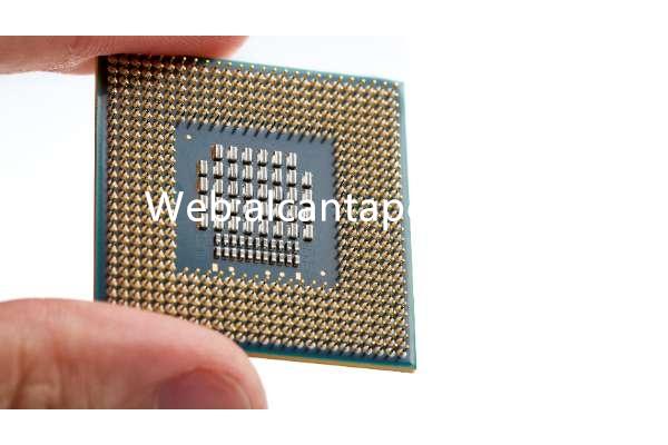
Что такое подложки для полупроводниковых стеклянных корпусов?
Подложка полупроводниковой стеклянной упаковки является одним из жизненно важных компонентов в современной электронной промышленности.. Это плоская пластинчатая конструкция, изготовленная из непроводящего материала., обычно стекловолокно, эпоксидная или композитная. Эти материалы обладают хорошими изоляционными свойствами и могут эффективно изолировать электрические сигналы между электронными компонентами., тем самым обеспечивая стабильную работу устройства.
На поверхности полупроводникового стекла упаковочный субстрат, точно проложены или напечатаны токопроводящие дорожки, которые называются линиями цепи. Компоновка линий схемы основана на функциональных требованиях к электронному оборудованию и связях между компонентами.. Эти линии не только обеспечивают электрические соединения между электронными компонентами., но также передавать сигналы данных и сигналы управления для обеспечения нормальной работы оборудования..
Процесс проектирования и производства подложек полупроводниковой стеклянной упаковки требует сложных технологий и оборудования.. В процессе производства, материал основы необходимо предварительно подготовить, а его поверхность должна быть ровной и гладкой. Затем, проводящие пути формируются на поверхности подложки с помощью методов химического травления или фотолитографии.. Следующий, отверстия в подложке делаются с помощью таких процессов, как сверление, для облегчения установки электронных компонентов.. Окончательно, такие операции, как сварка, нанесение покровного слоя, и проводятся испытания для завершения изготовления подложки полупроводниковой стеклянной упаковки..
Одним из основных преимуществ полупроводниковых стеклянных упаковочных подложек является их высокая надежность.. Благодаря прецизионному производственному процессу и материалам, эта подложка имеет стабильные электрические характеристики и хорошую механическую прочность., и может стабильно работать в течение длительного времени в различных суровых условиях. Кроме того, подложка полупроводниковой стеклянной упаковки также имеет меньший объем и вес, который может обеспечить легкий вес и миниатюризацию электронного оборудования и удовлетворить требования к объему и весу современного оборудования..
Общий, Подложки полупроводниковой стеклянной упаковки играют решающую роль в современной электронике.. Это не только носитель для подключения и поддержки электронных компонентов, но также является ключевым компонентом для обеспечения стабильной работы оборудования.. Благодаря постоянному развитию науки и техники и постоянному расширению областей применения., Подложки для полупроводниковой стеклянной упаковки будут продолжать играть важную роль в содействии развитию и инновациям электронной промышленности..
Справочное руководство по проектированию подложек стеклянных корпусов полупроводников.
Проектирование подложки полупроводниковой стеклянной упаковки является важной частью всего процесса разработки электронного продукта.. Он включает в себя компоновку электронных компонентов и прокладку схемных соединений, чтобы гарантировать, что конечный продукт функционирует и работает должным образом.. Существует множество факторов, которые необходимо учитывать в процессе проектирования, чтобы обеспечить производительность продукта., требования к надежности и изготовлению.
Первый, конструкторам необходимо разумно размещать электронные компоненты, включая чипсы, конденсаторы, индукторы, транзисторы, и т. д.. Разумное расположение компонентов может не только максимально сэкономить место и повысить компактность печатной платы., но также уменьшить помехи в цепи и улучшить целостность сигнала. В то же время, учитывая общий температурный режим продукта, проектировщикам также необходимо разумно расположить положения компонентов, чтобы добиться эффективного отвода тепла и обеспечить стабильность и надежность печатной платы во время работы..
Во-вторых, расположение линий соединения цепей должно быть тщательно продумано в процессе проектирования.. Хорошая конструкция проводки может минимизировать потери и помехи во время передачи сигнала и улучшить производительность и надежность схемы.. В процессе проводки, необходимо обратить внимание на расстояние между сигнальными линиями, линии электропередач, и линии заземления, чтобы избежать перекрестных помех и электромагнитных помех.. В то же время, направление и длина линий должны быть разумно спроектированы для обеспечения стабильности и скорости передачи сигнала..
В дополнение к размещению компонентов и маршрутизации цепей, дизайнерам также необходимо учитывать производственные требования и технологичность платы.. В процессе проектирования, необходимо соблюдать спецификации и стандарты производителя, чтобы гарантировать соответствие проектного решения требованиям реального производства.. Проектировщикам необходимо выбирать подходящие материалы и процессы, чтобы обеспечить качество и надежность печатной платы.. В то же время, производственные затраты и время цикла также должны быть приняты во внимание, чтобы обеспечить экономичность и практичность проектного решения..
Подводить итоги, Проектирование подложек полупроводниковой стеклянной упаковки включает в себя множество аспектов., включая компоновку компонентов, маршрутизация цепей, требования к терморегулированию и производству. Разумные конструктивные решения могут улучшить производительность и надежность продукта., сократить производственные затраты и циклы, и являются ключевым шагом в достижении целей проектирования электронных продуктов. Поэтому, дизайнерам необходимо полностью учитывать различные факторы и тщательно продумывать каждую деталь, чтобы конечный продукт мог соответствовать ожиданиям и потребностям пользователей..
Какой материал используется в подложках для полупроводниковых стеклянных корпусов??
Подложки полупроводниковой стеклянной упаковки являются важной частью современной электроники., и используемые материалы имеют решающее значение для их производительности и сферы применения.. Обычно, Подложки полупроводниковой стеклянной упаковки изготавливаются из таких материалов, как эпоксидная смола, армированная стекловолокном. (ФР4). FR4 имеет хорошие изоляционные свойства., механическая прочность и термостойкость, что делает его пригодным для большинства общих электронных приложений.
Однако, с постоянным развитием технологий и диверсификацией требований к применению, Выбор материалов для подложек полупроводниковой стеклянной упаковки также постоянно расширяется.. Другие материалы доступны в зависимости от конкретных требований применения., включая:
Керамика
Керамические подложки обладают превосходной термостойкостью и химической стабильностью., и подходят для применений в высокочастотных, высокая мощность и особые условия, такие как радиочастотные модули, усилители мощности и датчики.
Полиимид (ПИ)
Полиимидные подложки обладают превосходной стабильностью при высоких температурах., механическая прочность и химическая стойкость, что делает их пригодными для суровых условий в таких областях, как высокоскоростные цепи., аэрокосмическое и медицинское оборудование.
Металлическая основа
Подложки на металлической основе обычно изготавливаются из алюминия или меди, обладают отличными свойствами рассеивания тепла и подходят для мощных электронных устройств и светодиодного освещения..
Выбор этих различных материалов зависит от таких факторов, как требования к производительности продукта., условия эксплуатации и соображения стоимости. При выборе материалов, такие факторы, как теплопроводность, диэлектрическая проницаемость, механическая сила, стоимость и технологичность должны быть всесторонне рассмотрены, чтобы гарантировать, что производительность и надежность конечного продукта соответствуют ожидаемым целям..
Подводить итоги, Выбор материала подложки полупроводниковой стеклянной упаковки представляет собой комплексный процесс рассмотрения.. Разные материалы имеют свои преимущества и сферу применения., и соответствующий выбор может быть сделан в соответствии с конкретными требованиями приложения.
Какой размер имеют подложки для полупроводниковых стеклянных корпусов??
Размеры подложек полупроводниковой стеклянной упаковки варьируются в зависимости от конкретного применения и размера электронного устройства или системы.. Их размер может варьироваться от небольших подложек для мобильных телефонов и носимых устройств до больших подложек для промышленного оборудования и телекоммуникационной инфраструктуры..
Для небольших электронных устройств, таких как мобильные телефоны и носимые устройства., Подложки полупроводниковой стеклянной упаковки обычно должны быть очень компактными по размеру, чтобы адаптироваться к тенденции миниатюризации устройств.. На этих небольших подложках должны размещаться не только различные электронные компоненты., но также учтите легкость и портативность устройства. Как таковой, они часто имеют высокоинтегрированную конструкцию, которая достаточно мала, чтобы легко помещаться в ограниченном пространстве устройств..
Для больших систем, таких как промышленное оборудование и телекоммуникационная инфраструктура., размер подложки полупроводниковой стеклянной упаковки обычно больше. Эти большие подложки должны содержать больше электронных компонентов и сложные схемы, чтобы соответствовать требованиям высокой производительности устройства или системы.. Кроме того, при работе с большими подложками также необходимо учитывать такие вопросы, как рассеивание тепла и электромагнитная совместимость., поэтому размер обычно соответственно увеличивается.
Подложки для полупроводниковой стеклянной упаковки, будь то маленький или большой, должны быть точно спроектированы и изготовлены в соответствии с конкретными требованиями применения. В процессе проектирования, инженерам необходимо всесторонне учитывать такие факторы, как расположение электронных компонентов, пути передачи сигнала, эффекты рассеивания тепла, и механическая прочность, чтобы гарантировать, что окончательная конструкция подложки будет соответствовать требованиям к производительности и надежности продукта..
Поэтому подложки для полупроводниковой стеклянной упаковки выпускаются в широком диапазоне размеров., от нескольких миллиметров до десятков сантиметров, полностью в зависимости от размера и требований к производительности конкретных приложений и систем, которые они обслуживают..
Процесс изготовления подложек полупроводниковых стеклянных корпусов.
Процесс производства подложек для полупроводниковой стеклянной упаковки — это сложный и точный процесс, включающий множество важных этапов, обеспечивающих соответствие качества и характеристик конечного продукта ожидаемым стандартам.. Каждый аспект этого процесса будет подробно представлен ниже.:
Первый этап – подготовка субстрата.. На этом этапе, подбирается подложка подходящего размера и материала, обычно эпоксидная смола, армированная стекловолокном (ФР4) или другие специфические материалы. Подложки должны подвергаться тщательной очистке и обработке поверхности, чтобы обеспечить плавное продвижение на последующих этапах процесса..
Далее выравнивание слоев. На этом этапе, различные слои подложки выровнены, чтобы обеспечить правильную компоновку и соединение дорожек схемы.. Это требует высокоточного оборудования и деликатных операций, чтобы гарантировать точность положения и ориентации каждого слоя..
Затем следует травление или печать линий схемы.. На этом решающем этапе, Для формирования проводящих путей используются методы химического травления или печати., то есть, линии цепи, на поверхности подложки, в зависимости от требований к проектированию. Эти пути будут путями, соединяющими электронные компоненты., поэтому их качество и точность имеют решающее значение.
Далее следует сверление отверстий для компонентов.. На этом этапе, высокоточное сверлильное оборудование используется для сверления отверстий в подложке для монтажа электронных компонентов. Расположение и размер отверстий должны точно контролироваться, чтобы обеспечить возможность точной установки и подключения компонентов к дорожкам цепи..
Затем следует наложение накладки на площадку.. На этом этапе, на подложку наносится накладка для пайки электронных компонентов. Качество контактной площадки и однородность покрытия имеют решающее значение для качества пайки., требующие точного контроля процесса и высококачественных материалов.
Далее идет сборка компонентов. На этом этапе, электронные компоненты аккуратно монтируются на подложку в соответствии с требованиями дизайна и фиксируются с помощью пайки или других методов крепления.. Правильная установка и подключение компонентов является ключевым фактором обеспечения работоспособности конечного продукта..
Окончательно, идет этап тестирования. На этом этапе, Собранная подложка полупроводниковой стеклянной упаковки подвергается всесторонним функциональным испытаниям и оценке производительности.. Сюда входят электрические испытания, проверка целостности сигнала, термические испытания, и многое другое, чтобы гарантировать, что продукт соответствует спецификациям и имеет хорошую надежность..
Благодаря вышеуказанной серии строгих производственных этапов, Подложки для полупроводниковой стеклянной упаковки могут обеспечить высокое качество, высокопроизводительное производство, обеспечение надежной поддержки и гарантии нормальной работы различного электронного оборудования и систем.
Область применения подложек полупроводниковых стеклянных корпусов.
Подложки полупроводниковой стеклянной упаковки сегодня играют незаменимую роль в различных отраслях промышленности мира.. Их широкий спектр применения простирается от бытовой электроники до промышленной автоматизации.. Первый, давайте посмотрим на сектор бытовой электроники. В этой области, Подложки полупроводниковой стеклянной упаковки широко используются в таких продуктах, как смартфоны., таблетки, умные домашние устройства, и личные электронные аксессуары. Конструкция этих продуктов требует небольших, эффективные печатные платы, и подложки для полупроводниковой стеклянной упаковки идеально подходят для удовлетворения этих потребностей..
В автомобильной промышленности, Подложки полупроводниковой стеклянной упаковки также играют ключевую роль. Современные системы управления автомобилем включают в себя сложные электронные блоки управления. (КРЫШКА) которые управляют управлением двигателем, развлечения в машине, системы безопасности и функции помощи водителю. Этим блокам управления требуются высоконадежные печатные платы для поддержки их функций., и полупроводниковые стеклянные упаковочные подложки могут обеспечить стабильные электрические соединения и отличные характеристики для обеспечения надежной работы автомобильных систем..
Аэрокосмическая отрасль также является одной из важных областей применения полупроводниковых стеклянных упаковочных материалов.. Электронные системы самолетов и космических аппаратов предъявляют строгие требования к экстремальным условиям, таким как высокая температура., высокое давление и сильная вибрация. Подложки полупроводниковой стеклянной упаковки могут обеспечить превосходную устойчивость к высоким температурам и вибрации., поэтому они широко используются в производстве аэрокосмического электронного оборудования..
Область медицинского оборудования является еще одной важной областью применения.. От кардиостимуляторов до медицинского оборудования для визуализации, современные медицинские устройства требуют высоконадежных электронных компонентов для обеспечения их безопасности и точности.. Подложки полупроводниковой стеклянной упаковки могут обеспечить стабильные электрические характеристики и надежные соединения., удовлетворение требований медицинского оборудования к качественным электронным компонентам.
Кроме того, области телекоммуникаций и промышленной автоматизации также являются одной из основных областей применения полупроводниковых стеклянных упаковочных подложек.. Будь то обработка сигналов для коммуникационного оборудования или системы управления промышленными роботами., эти приложения полагаются на стабильные и надежные печатные платы для реализации своих функций..
Общий, Подложки для полупроводниковой стеклянной упаковки играют важную роль в различных отраслях промышленности., обеспечение стабильной и надежной основы для современных электронных устройств и систем. Благодаря постоянному развитию технологий, Считается, что подложки для полупроводниковой стеклянной упаковки будут продолжать играть ключевую роль в будущей электронной сфере..
Каковы преимущества подложек полупроводниковых стеклянных корпусов??
Подложки для полупроводниковой стеклянной упаковки, в качестве ключевых компонентов современной электроники, предлагают множество существенных преимуществ по сравнению с другими методами проводки. Первый, их компактный размер позволяет делать электронные устройства тоньше, легче, и меньше, тем самым удовлетворяя потребности современной бытовой электроники в легкости и портативности.. Кроме того, высокая надежность подложек полупроводниковых стеклянных упаковок является еще одним важным преимуществом их популярности.. Подложки, изготовленные из таких материалов, как эпоксидная смола, армированная стекловолокном, обладают превосходными физическими свойствами и могут выдерживать высокие температуры и давление окружающей среды., тем самым обеспечивая стабильность и долговечность электронных устройств.
Еще одним важным преимуществом полупроводниковых стеклянных упаковочных подложек является простота их массового производства.. По сравнению с традиционными методами, такими как ручная проводка, Процесс производства подложек полупроводниковой стеклянной упаковки может быть реализован с помощью автоматизированного оборудования и операций сборочной линии., что значительно повышает эффективность производства и снижает производственные затраты, делая возможным массовое производство.
Кроме того, Подложки для полупроводниковой стеклянной упаковки могут значительно снизить вероятность ошибок при сборке.. Благодаря точному проектированию и производственным процессам, электронные компоненты могут быть точно и надежно закреплены на подложке, снижение вероятности выхода из строя и повреждений, вызванных неправильной сборкой, а также повышение качества и надежности продукции..
Кроме того, Подложки полупроводниковой стеклянной упаковки также могут улучшить целостность сигнала и гарантировать, что электронные устройства смогут поддерживать стабильность и точность сигнала при передаче данных.. Путем оптимизации конструкции и проводки, помехи сигнала и перекрестные помехи могут быть уменьшены, а качество и скорость передачи сигнала можно улучшить, тем самым улучшая производительность всей системы.
Окончательно, Подложки для полупроводниковой стеклянной упаковки также обладают хорошими термическими свойствами.. Поскольку такие материалы, как эпоксидная смола, армированная стекловолокном, обладают хорошей теплопроводностью., подложка полупроводниковой стеклянной упаковки может эффективно рассеивать тепло, предотвратить повреждение электронных компонентов из-за перегрева, и продлить срок службы оборудования.
В итоге, Подложки для полупроводниковой стеклянной упаковки имеют множество преимуществ, таких как компактный размер., высокая надежность, удобное массовое производство, уменьшение ошибок сборки, улучшенная целостность сигнала, и хорошие тепловые характеристики, что делает их незаменимой частью современного электронного оборудования.. компонент.
Часто задаваемые вопросы
В чем разница между подложкой полупроводниковой стеклянной упаковки и традиционной печатной платой??
Подложки полупроводниковой стеклянной упаковки обычно изготавливаются из специальных материалов, таких как эпоксидная смола, армированная стекловолокном., которые характеризуются высокой температурной устойчивостью и отличной теплопроводностью.. По сравнению с традиционной печатной платой FR4, Подложки полупроводниковой стеклянной упаковки лучше справляются с высокими температурами и требованиями к рассеиванию тепла..
Каковы ключевые этапы процесса производства подложек полупроводниковой стеклянной упаковки??
Ключевые этапы производства подложек для полупроводниковой стеклянной упаковки включают подготовку подложек., выравнивание слоев, травление или печать линий схемы, сверление отверстий под детали, нанесение чехла на подушку, сборка и тестирование компонентов, и т. д.. Каждый шаг имеет решающее значение и влияет на качество и производительность конечного продукта..
В каких областях широко используются полупроводниковые стеклянные упаковочные подложки?
Подложки полупроводниковой стеклянной упаковки широко используются в бытовой электронике., автомобили, медицинское оборудование, оборудование связи и другие области. Например, они используются для производства критически важных продуктов, таких как смартфоны., автомобильные электронные системы, медицинское оборудование для визуализации, и инфраструктура связи.
Какое программное обеспечение для проектирования подложек полупроводниковой стеклянной упаковки??
Программное обеспечение, обычно используемое для проектирования подложек полупроводниковой стеклянной упаковки, включает Altium Designer., Каденс Аллегро, Наставник графики, и т. д.. Это программное обеспечение предоставляет богатый набор функций и инструментов для поддержки пользователей в эффективном проектировании и компоновке схем..
Насколько надежна полупроводниковая стеклянная упаковочная подложка?
Подложки полупроводниковой стеклянной упаковки обладают высокой надежностью и могут стабильно работать в различных условиях окружающей среды.. Ее материалы и производственные процессы тщательно разработаны в соответствии со строгими промышленными стандартами и требованиями., обеспечение долгосрочной стабильности и надежности продукта.