CO.,LTD")
Hersteller von Halbleiter-Lastplatinen. Ein Hersteller von Halbleiter-Lastplatinen ist auf die Herstellung von Lastplatinen zum Testen von Halbleiterbauelementen spezialisiert. Diese Ladetafeln dienen als wichtige Vermittler, Anschließen von Halbleiterkomponenten an Testgeräte. Sie gewährleisten eine genaue und zuverlässige Prüfung integrierter Schaltkreise (ICs) durch die Bereitstellung der notwendigen elektrischen Verbindungen und die Erleichterung der Signalübertragung. Hochwertige Lastbretter sind so konzipiert, dass sie präzise Spezifikationen erfüllen und strengen Testbedingungen standhalten, Damit sind sie unverzichtbar für die Bewertung der Leistung und Funktionalität von Halbleiterbauelementen, bevor sie in Endprodukte integriert werden.
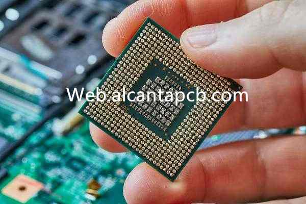
Halbleiter-Lastplatinen sind wichtige Komponenten im Test- und Validierungsprozess von Halbleiterbauelementen. Diese Platinen sind speziell für den Anschluss von Halbleiterbauelementen konzipiert, wie integrierte Schaltkreise (ICs) und andere Chips, bis hin zu automatisierten Testgeräten (ASS) Systeme. Die Lastplatine dient als Schnittstelle zwischen dem ATE und dem zu testenden Gerät (Ich habe), Dies ermöglicht eine genaue Beurteilung der elektrischen Eigenschaften des Geräts, Leistung, und Funktionalität unter verschiedenen Bedingungen. In diesem Artikel, Wir werden das Design untersuchen, Materialien, Herstellungsprozesse, und Anwendungen von Halbleiter-Lastplatinen, Dies unterstreicht ihre Bedeutung in der Halbleitertestbranche.
Was ist ein Halbleiter-Lastboard??
Eine Halbleiter-Lastplatine ist eine spezielle Leiterplatte (Leiterplatte) Wird in der Halbleitertestindustrie verwendet. Sein Hauptzweck besteht darin, die Verbindung zwischen einem Halbleiterbauelement zu erleichtern (der Prüfling) und die automatisierten Testgeräte (ASS) Dies wird zur Bewertung der Leistung des Geräts verwendet. Die Lastplatine ist mit Präzision konstruiert, um sicherzustellen, dass sie die Betriebsumgebung des Halbleiterbauelements genau nachbildet, Dies ermöglicht umfassende Tests und Validierungen.
Load Boards werden auf die spezifischen Anforderungen des Prüflings zugeschnitten, unter Berücksichtigung von Faktoren wie der Pin-Konfiguration, Signalintegrität, Leistungsabgabe, und Wärmemanagement. Das Design einer Lastplatine muss sicherstellen, dass sie die Hochgeschwindigkeitssignale und Leistungsanforderungen moderner Halbleiterbauelemente bewältigen kann, während gleichzeitig die Signalintegrität gewahrt bleibt und Rauschen und Interferenzen minimiert werden.
Die Komplexität einer Halbleiter-Lastplatine hängt von der Art des zu prüfenden Geräts und dem Umfang der Prüfung ab. Zum Beispiel, Lastplatinen zum Testen fortschrittlicher Mikroprozessoren oder System-on-Chips (SoCs) kann eine komplizierte Streckenführung erfordern, mehrere Schichten, und die Integration passiver und aktiver Komponenten, um die Betriebsbedingungen des DUT genau zu simulieren. Im Gegensatz, Lastplatinen für einfachere ICs sind möglicherweise weniger komplex, erfordern aber dennoch eine sorgfältige Konstruktion, um genaue Tests zu gewährleisten.
Design und Materialien
Das Design einer Halbleiter-Lastplatine ist ein entscheidender Aspekt ihrer Funktionalität. Ingenieure müssen verschiedene Faktoren berücksichtigen, inklusive der Elektrik, mechanisch, und thermische Eigenschaften der Platine, um sicherzustellen, dass es die Testanforderungen des DUT erfüllt.
Der elektrische Entwurf einer Lastplatine erfordert die sorgfältige Anordnung der Leiterbahnen, Durchkontaktierungen, und Komponenten zur Gewährleistung der Signalintegrität, kontrollierte Impedanz, und eine ordnungsgemäße Stromverteilung. Hohe Geschwindigkeit Signale müssen präzise weitergeleitet werden, um Übersprechen und elektromagnetische Störungen zu minimieren (EMI). Ingenieure müssen auch die Platzierung von Entkopplungskondensatoren berücksichtigen, Widerstände, und andere passive Komponenten zur Stabilisierung der Stromversorgung und Reduzierung von Geräuschen.
Beim mechanischen Design eines Loadboards steht der physische Aufbau im Mittelpunkt, einschließlich der Platzierung von Anschlüssen, Steckdosen, und Befestigungslöcher. Die Platine muss so ausgelegt sein, dass sie den Prüfling während des Tests sicher an Ort und Stelle hält, Gewährleistung zuverlässiger Verbindungen zwischen dem DUT und dem ATE. Das mechanische Design berücksichtigt auch die Haltbarkeit des Boards, da Lastplatinen häufig wiederholten Testzyklen unterzogen werden.
Beim Design von Halbleiter-Lastplatinen ist das Wärmemanagement von entscheidender Bedeutung, insbesondere für Geräte, die beim Testen erhebliche Wärmemengen erzeugen. Ingenieure können Kühlkörper einbauen, thermische Durchkontaktierungen, und andere Kühlmechanismen in das Lastplatinendesign integriert, um Wärme abzuleiten und eine Überhitzung des Prüflings zu verhindern.
Die für die Konstruktion eines Lastbretts verwendeten Materialien werden auf der Grundlage der spezifischen Anforderungen des Testprozesses ausgewählt. Zu den gängigen Materialien gehört hochwertiges FR4, BT Harz, und andere fortschrittliche Laminate, die hervorragende elektrische und thermische Eigenschaften bieten. Die Wahl des Materials beeinflusst auch die Fähigkeit des Boards, hohe Frequenzen zu verarbeiten, Signalintegrität, und Wärmemanagement.
Herstellungsprozess
Der Herstellungsprozess einer Halbleiter-Lastplatine umfasst mehrere wichtige Schritte, Jedes davon muss sorgfältig kontrolliert werden, um die Leistung und Zuverlässigkeit des Boards sicherzustellen.
Der Herstellungsprozess beginnt mit der Vorbereitung der Grundmaterialien, inklusive der Auswahl an Laminaten, Kupferfolien, und andere Materialien, die die Schichten der Platte bilden. Diese Materialien werden basierend auf der Elektrik ausgewählt, mechanisch, und thermische Anforderungen der Lastplatine.
Halbleiter-Lastplatinen bestehen häufig aus mehreren Schichten, Jedes davon ist zu einer einzigen Platte laminiert. Der Schichtungsprozess umfasst die präzise Ausrichtung der Schichten, um sicherzustellen, dass die Leiterbahnen und Durchkontaktierungen auf jeder Schicht korrekt verbunden sind. Die Schichten werden dann unter hohem Druck und hoher Temperatur laminiert, um eine starke Verbindung zu schaffen, langlebiges Brett.
Nach dem Laminieren, Löcher werden in die Platine gebohrt, um Durchkontaktierungen zu erzeugen, die dann mit Kupfer plattiert werden, um elektrische Verbindungen zwischen den Schichten herzustellen. Der Bohrvorgang muss äußerst präzise sein, um sicherzustellen, dass die Durchkontaktierungen korrekt mit den Leiterbahnen auf jeder Schicht übereinstimmen.
Der nächste Schritt umfasst die Strukturierung der Kupferschichten, um die Leiterbahnen und Pads zu erstellen, die die elektrischen Signale übertragen. Dies erfolgt typischerweise mittels Fotolithographie, Dabei wird ein Fotolack auf die Kupferoberfläche aufgetragen, UV-Licht ausgesetzt, und dann entwickelt, um das gewünschte Muster zu erstellen. Das freigelegte Kupfer wird dann weggeätzt, hinterlässt Spuren und Beläge.
Zum Schutz der Leiterbahnen und zur Vermeidung von Lötbrücken während des Montageprozesses wird eine Lötstoppmaske aufgetragen. Zusätzlich erhält die Platte eine Oberflächenveredelung, wie Hasl (Heißluft-Lotnivellierung) oder ENIG (Chemisches Nickel-Immersionsgold), zum Schutz der Kupferpads und zur Verbesserung der Lötbarkeit.
Sobald die Platine gefertigt ist, Komponenten wie Steckdosen, Anschlüsse, und passive Komponenten werden auf der Platine montiert. Dieser Prozess kann sowohl Oberflächenmontage- als auch Durchstecklöttechniken umfassen, abhängig vom Design der Platine.
Der letzte Schritt im Herstellungsprozess ist die Prüfung und Qualitätskontrolle. Das Board wird verschiedenen Tests unterzogen, einschließlich elektrischer Prüfungen, thermische Prüfung, und mechanische Inspektion, um sicherzustellen, dass es den geforderten Spezifikationen entspricht und frei von Mängeln ist.
Anwendungen von Halbleiter-Lastplatinen
Halbleiter-Lastplatinen werden in einer Vielzahl von Anwendungen in der Halbleiterindustrie eingesetzt, insbesondere beim Testen und Validieren von Halbleiterbauelementen. Zu den wichtigsten Anwendungen gehören:
Load Boards werden beim Testen auf Waferebene eingesetzt, Hier werden Halbleiterbauelemente getestet, bevor sie vom Wafer getrennt werden. Bei diesem Vorgang wird die Ladeplatine mit einer Wafer-Sonde-Card verbunden, Dies stellt den Kontakt zu den Geräten auf dem Wafer her und ermöglicht elektrische Tests.
In der letzten Testphase, Lastplatinen werden verwendet, um vollständig verpackte Halbleiterbauelemente zu testen, bevor sie an Kunden ausgeliefert werden. Diese Phase ist entscheidend, um sicherzustellen, dass die Geräte den erforderlichen Spezifikationen entsprechen und frei von Mängeln sind.
Beim Burn-In-Test werden Halbleiterbauelemente erhöhten Temperaturen und Spannungen ausgesetzt, um den Langzeitgebrauch zu simulieren und frühzeitige Ausfälle zu erkennen. Bei Burn-In-Tests verwendete Lastplatinen müssen so konstruiert sein, dass sie diesen rauen Bedingungen standhalten und gleichzeitig zuverlässige Verbindungen zum Prüfling aufrechterhalten.
Lastplatinen werden auch bei Qualifikations- und Zuverlässigkeitstests eingesetzt, Hier werden Halbleiterbauelemente unter verschiedenen Bedingungen getestet, um ihre Leistung zu bewerten, Zuverlässigkeit, und Haltbarkeit im Laufe der Zeit. Diese Tests sind unerlässlich, um sicherzustellen, dass die Geräte in ihren vorgesehenen Anwendungen zuverlässig funktionieren.
FAQ
Was ist die Hauptfunktion einer Halbleiter-Lastplatine??
Eine Halbleiter-Lastplatine dient als Schnittstelle zwischen dem Prüfling (Ich habe) und die automatisierten Testgeräte (ASS), Dies erleichtert die genaue Beurteilung der elektrischen Eigenschaften des Geräts, Leistung, und Funktionalität.
Welche Faktoren werden bei der Gestaltung eines Lastbretts berücksichtigt??
Zu den Schlüsselfaktoren gehört das elektrische Design für die Signalintegrität, Mechanisches Design für sichere Verbindungen, Thermomanagement zur Vermeidung von Überhitzung, und die Auswahl der Materialien basiert auf den elektrischen und thermischen Anforderungen der Platine.
Welche Materialien werden üblicherweise in Halbleiter-Lastplatinen verwendet??
Zu den gängigen Materialien gehört hochwertiges FR4, BT Harz, und fortschrittliche Laminate, die hervorragende elektrische und thermische Eigenschaften bieten, Gewährleistung einer zuverlässigen Leistung während des Tests.
In welchen Anwendungen werden Halbleiter-Lastplatinen eingesetzt??
Halbleiter-Lastplatinen werden beim Testen auf Waferebene eingesetzt, Abschlusstest, Burn-in-Test, sowie Qualifikations- und Zuverlässigkeitstests, spielen eine entscheidende Rolle im Halbleiterherstellungsprozess.