CO.,LTD")
Hersteller von Halbleitersubstraten. Ein Hersteller von Halbleitersubstraten ist auf die Herstellung wesentlicher Komponenten für die Halbleiterindustrie spezialisiert. Diese Hersteller stellen hochwertige Substrate bereit, die als Grundschicht für Halbleiterbauelemente dienen. Ihr Fachwissen umfasst die Herstellung von Substraten aus verschiedenen Materialien, wie z.B. Silizium, Keramik, Und Hochfrequenz Laminate, auf spezifische Leistungsanforderungen zugeschnitten. Sie gewährleisten Präzision in Design- und Herstellungsprozessen, um fortschrittliche Anwendungen in der Elektronik zu unterstützen, Telekommunikation, und Automotive-Bereiche, Dies treibt letztendlich Innovation und Zuverlässigkeit in der Halbleitertechnologie voran.
Halbleitersubstrate sind Grundmaterialien, auf denen integrierte Schaltkreise basieren (ICs) werden fabriziert, spielen eine entscheidende Rolle für die Leistung und Funktionalität moderner Elektronik. Diese Substrate dienen als Basis für Halbleiterbauelemente, wie Transistoren, Dioden, und integrierte Schaltkreise, werden gebaut. Die Qualität und Eigenschaften eines Halbleiters Substrat die elektrische Leistung erheblich beeinflussen, Wärmemanagement, und Gesamtzuverlässigkeit der elektronischen Komponenten, die es unterstützt. In diesem Artikel werden die verschiedenen Aspekte von Halbleitersubstraten untersucht, einschließlich ihrer Materialien, Eigenschaften, Herstellungsprozesse, Anwendungen, und die Vorteile, die sie der Elektronikindustrie bieten.
Was ist ein Halbleitersubstrat??
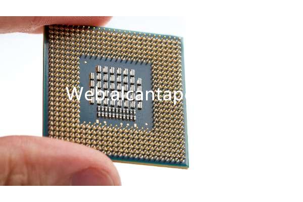
Ein Halbleitersubstrat ist ein Material, typischerweise ein Wafer, das eine Oberfläche für die Herstellung von Halbleiterbauelementen bietet. Das Substrat fungiert als physischer Träger für die Gerätestrukturen und als elektrische Leitung, Erleichterung des Signal- und Stromflusses innerhalb des Geräts. Halbleitersubstrate bestehen üblicherweise aus Silizium, aber auch andere Materialien wie Galliumarsenid (GaAs), Siliziumkarbid (SiC), und Indiumphosphid (InP) werden auch verwendet, abhängig von den spezifischen Anwendungsanforderungen. Die Wahl des Substratmaterials beeinflusst die elektrischen Eigenschaften der Geräte, wie Geschwindigkeit, Stromverbrauch, und Wärmeableitung, Dies macht es zu einer entscheidenden Komponente im Halbleiterherstellungsprozess.
Eigenschaften von Halbleitersubstraten
Halbleitersubstrate verfügen über mehrere Schlüsseleigenschaften, die ihre Eignung für verschiedene Anwendungen bestimmen:
Die Leitfähigkeit des Substratmaterials ist eine grundlegende Eigenschaft, die die Leistung der Halbleiterbauelemente beeinflusst. Silizium, das gebräuchlichste Substratmaterial, ist ein Halbleiter mit mäßiger Leitfähigkeit, während Materialien wie GaAs und InP eine höhere Elektronenmobilität bieten, Dadurch sind sie für Hochfrequenz- und optoelektronische Anwendungen geeignet.
Die Fähigkeit des Substrats, Wärme abzuleiten, ist entscheidend für die Aufrechterhaltung der Leistung und Langlebigkeit von Halbleiterbauelementen. Materialien wie SiC sind für ihre hohe Wärmeleitfähigkeit bekannt, Damit eignen sie sich ideal für Leistungselektronik und Hochtemperaturanwendungen.
Das Substrat muss eine ausreichende mechanische Festigkeit aufweisen, um die Herstellungsprozesse zu unterstützen, wie Lithographie, Radierung, und Ablagerung, ohne zu brechen oder sich zu verziehen. Dies ist besonders wichtig bei fortschrittlichen Verpackungstechniken, bei denen die Substrate verdünnt werden, um die Gesamtdicke des Geräts zu reduzieren.
Die Oberfläche des Halbleitersubstrats muss extrem glatt und fehlerfrei sein, um eine ordnungsgemäße Herstellung des Geräts zu gewährleisten. Jegliche Unvollkommenheiten auf der Substratoberfläche können zu Defekten in den Halbleiterbauelementen führen, Auswirkungen auf ihre Leistung und ihren Ertrag haben.
Das Substratmaterial muss mit den bei der Herstellung von Halbleiterbauelementen verwendeten Prozessen kompatibel sein, einschließlich Doping, Oxidation, und Metallisierung. Diese Kompatibilität stellt sicher, dass die Geräte zuverlässig mit den gewünschten elektrischen Eigenschaften hergestellt werden können.
Materialien, die in Halbleitersubstraten verwendet werden
Als Halbleitersubstrate werden verschiedene Materialien verwendet, Jedes bietet unterschiedliche Vorteile für bestimmte Anwendungen:
Silizium ist aufgrund seiner reichlichen Verfügbarkeit das am häufigsten verwendete Halbleitersubstratmaterial, etablierte Herstellungsprozesse, und vielseitige elektrische Eigenschaften. Es wird in einer Vielzahl von Anwendungen eingesetzt, von Mikroprozessoren und Speicherchips bis hin zu Leistungsgeräten und Sensoren.
GaAs-Substrate sind für ihre hohe Elektronenmobilität und direkte Bandlücke bekannt, Damit sind sie ideal für Hochfrequenz- und optoelektronische Anwendungen, wie HF-Verstärker, Laser, und Solarzellen.
SiC-Substrate bieten eine hervorragende Wärmeleitfähigkeit und mechanische Festigkeit, Dadurch sind sie für Hochleistungs- und Hochtemperaturanwendungen geeignet, wie zum Beispiel Elektrofahrzeuge, Leistungswandler, und Luft- und Raumfahrtelektronik.
InP-Substrate werden in Hochgeschwindigkeits- und optoelektronischen Geräten verwendet, wie Fotodetektoren und Laserdioden, aufgrund ihrer hervorragenden Elektronenmobilität und Hochfrequenzleistung.
Saphirsubstrate werden aufgrund ihrer Transparenz vor allem in der Optoelektronik und bei LED-Anwendungen eingesetzt, hohe Wärmeleitfähigkeit, und mechanische Festigkeit.
Herstellungsprozess von Halbleitersubstraten
Die Herstellung von Halbleitersubstraten umfasst mehrere entscheidende Schritte, um die Qualität und Leistung des Endprodukts sicherzustellen:
Der Prozess beginnt mit dem Wachstum eines großen Einkristalls, als Boule bekannt, aus dem Rohmaterial. Für Siliziumsubstrate, Dies erfolgt typischerweise nach dem Czochralski-Verfahren, Dabei wird ein Impfkristall in geschmolzenes Silizium getaucht und langsam herausgezogen, um einen zylindrischen Kristall zu bilden.
Anschließend wird die Kugel mit einer Diamantdrahtsäge in dünne Scheiben geschnitten. Die Dicke der Wafer kann je nach Anwendung variieren, aber sie liegen typischerweise dazwischen 150 Zu 300 Mikrometer dick.
Die geschnittenen Wafer durchlaufen eine Reihe von Polierschritten, um eine spiegelähnliche Oberfläche zu erzielen. Dieser Schritt ist entscheidend, um sicherzustellen, dass die Oberfläche des Substrats glatt und frei von Fehlern ist, Dies ist für die Herstellung von Geräten mit hoher Ausbeute unerlässlich.
Die Wafer können mit Verunreinigungen dotiert werden, um ihre elektrischen Eigenschaften zu verändern. Durch Dotierung werden Atome anderer Elemente eingeführt, wie Bor oder Phosphor, in den Untergrund, Es entstehen Bereiche mit n- oder p-Leitfähigkeit.
Die Wafer können auch oxidiert werden, wodurch eine dünne Schicht Siliziumdioxid auf der Oberfläche entsteht, Es dient als Isolator und schützt das Substrat vor Verunreinigungen bei der Weiterverarbeitung.
Die fertigen Substrate werden auf Mängel untersucht, wie zum Beispiel Risse, Gruben, oder Verrenkungen, und auf elektrische Eigenschaften geprüft. Bei der Herstellung von Halbleiterbauelementen werden nur Wafer verwendet, die strengen Qualitätsstandards entsprechen.
Anwendungen von Halbleitersubstraten
Halbleitersubstrate sind ein wesentlicher Bestandteil einer Vielzahl von Anwendungen in der modernen Elektronik:
Siliziumsubstrate bilden die Basis für die in Computern verwendeten Mikroprozessoren und Speicherchips, Smartphones, und andere digitale Geräte. Die Zuverlässigkeit und Skalierbarkeit von Silizium machen es ideal für diese großvolumigen Anwendungen.
SiC-Substrate werden zunehmend in der Leistungselektronik eingesetzt, wie zum Beispiel Wechselrichter, Konverter, und Motorantriebe, aufgrund ihrer Fähigkeit, hohe Spannungen und Temperaturen mit minimalem Energieverlust zu bewältigen.
GaAs- und InP-Substrate sind für HF- und Mikrowellengeräte unerlässlich, inklusive Verstärker, Oszillatoren, und Transceiver, wo die Hochfrequenzleistung entscheidend ist.
Substrate wie GaAs, InP, und Saphir werden bei der Herstellung optoelektronischer Geräte verwendet, inklusive LEDs, Laserdioden, und Fotodetektoren, die Materialien mit spezifischen optischen und elektronischen Eigenschaften erfordern.
Halbleitersubstrate werden auch in einer Vielzahl von Sensoren und Aktoren verwendet, einschließlich Drucksensoren, Beschleunigungsmesser, und Gyroskope, die man im Automobilbereich findet, industriell, und Verbraucheranwendungen.
Vorteile von Halbleitersubstraten
Die Verwendung von Halbleitersubstraten bietet mehrere Vorteile bei der Herstellung elektronischer Geräte:
Die elektrischen Eigenschaften von Halbleitersubstraten, wie Elektronenmobilität und Wärmeleitfähigkeit, tragen direkt zur Leistung der darauf gefertigten Geräte bei.
Halbleitersubstrate, insbesondere Silizium, eignen sich gut für die Großserienfertigung, Dies ermöglicht die Produktion von Milliarden von Geräten mit gleichbleibender Qualität und Leistung.
Die Kompatibilität von Halbleitersubstraten mit verschiedenen Herstellungsprozessen ermöglicht die Integration mehrerer Geräte auf einem einzigen Chip, Reduzierung der Größe, kosten, und Stromverbrauch.
Die mechanische Festigkeit und thermische Stabilität von Halbleitersubstraten gewährleisten die Haltbarkeit und Zuverlässigkeit der Geräte unter verschiedenen Betriebsbedingungen.
FAQ
Wofür werden Halbleitersubstrate verwendet??
Halbleitersubstrate dienen als Grundmaterial für die Herstellung von Halbleiterbauelementen, wie Transistoren, Dioden, und integrierte Schaltkreise. Sie werden in einer Vielzahl von Anwendungen eingesetzt, einschließlich Mikroprozessoren, Leistungselektronik, HF-Geräte, und Optoelektronik.
Warum ist Silizium das am häufigsten verwendete Halbleitersubstratmaterial??
Silizium ist aufgrund seiner Häufigkeit das am häufigsten vorkommende Halbleitersubstratmaterial, Wirtschaftlichkeit, und etablierte Herstellungsprozesse. Seine elektrischen Eigenschaften machen es vielseitig für eine Vielzahl von Anwendungen, von digitaler Logik bis hin zu Leistungsgeräten.
Welche Vorteile bietet die Verwendung von Siliziumkarbid? (SiC) Substrate?
SiC-Substrate bieten eine hohe Wärmeleitfähigkeit, mechanische Festigkeit, und die Fähigkeit, bei hohen Spannungen und Temperaturen zu arbeiten, Damit eignen sie sich ideal für Leistungselektronik und Hochtemperaturanwendungen.
Wie werden Halbleitersubstrate hergestellt??
Der Herstellungsprozess von Halbleitersubstraten beinhaltet das Kristallwachstum, Waffeln schneiden, Oberflächenpolieren, Doping, Oxidation, und strenge Inspektionen und Tests, um Qualität und Leistung sicherzustellen.