КОМПАНИЯ С ОГРАНИЧЕННОЙ ОТВЕТСТВЕННОСТЬЮ")
Производитель процессов упаковки SIP. (Система в пакете) упаковка производитель процессов специализируется на интеграции нескольких микросхем, пассивные компоненты, и другие элементы в один пакет, Оптимизация пространства и производительности. Эти производители используют расширенные методы для обеспечения точной сборки, Эффективное тепловое управление, и надежные электрические соединения, обслуживание высокопроизводительных приложений в таких отраслях, как телекоммуникации, автомобильный, и бытовая электроника. Их опыт позволяет создавать компактные, многофункциональные пакеты, отвечающие требованиям современных технологий, стимулирование инноваций и эффективности в электронных устройствах.
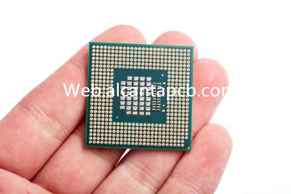
ГЛОТОК (Система в пакете) упаковка — это передовая технология упаковки полупроводников, объединяющая несколько интегральных схем. (ИС) и пассивные компоненты в одном корпусе, предоставление компактного и эффективного решения для электронных систем. Процесс упаковки SIP имеет решающее значение для миниатюризации электронных устройств., улучшение производительности, и снижение энергопотребления. Этот процесс широко используется в таких приложениях, как смартфоны., IoT-устройства, и носимые технологии, где пространство и энергоэффективность имеют первостепенное значение.
Что такое SIP-упаковка?
SIP-упаковка предполагает интеграцию нескольких полупроводниковых компонентов, таких как процессоры., чипы памяти, датчики, и пассивные элементы — в один модуль. Эти компоненты взаимосвязаны внутри пакета и функционируют как целостная система., часто включая различные типы микросхем, выполняющих различные функции. SIP могут включать в себя различные типы пакетов., включая флип-чип, проволочный, и через кремний через (ТСВ) технологии, в зависимости от конкретных требований приложения.
Основным преимуществом SIP-упаковки является ее способность сочетать несколько функций в компактном форм-факторе., позволяющая развивать более мелкие, легче, и более эффективные электронные устройства. Путем интеграции компонентов на уровне пакета, Технология SIP также позволяет улучшить электрические характеристики., более короткие пути прохождения сигнала, и снижение энергопотребления, что делает его идеальным для высокопроизводительных и маломощных приложений..
Этапы процесса упаковки SIP
Процесс SIP-упаковки включает в себя несколько важных этапов., каждый из которых необходим для обеспечения надежности, производительность, и эффективность конечного продукта. Этот процесс можно разделить на следующие ключевые этапы.:
Процесс упаковки SIP начинается с этапа проектирования и планирования., где инженеры определяют спецификации, архитектура, и расположение SIP. Это включает в себя выбор компонентов, которые будут интегрированы., определение стратегии межсетевого взаимодействия, и разработка компоновки упаковки для оптимизации производительности и минимизации размера.. Этап проектирования также включает моделирование и моделирование для прогнозирования тепловых характеристик., механический, и электрическое поведение SIP.
Как только дизайн будет завершен, отдельный полупроводник умирает (ИС) готовы к интеграции. Это включает в себя утончение пластины, игра в кости, и осмотр. Утончение пластин уменьшает толщину штампов, позволяющая получить более компактный пакет. Нарезка кубиками включает в себя разрезание пластины на отдельные матрицы., которые затем проверяются на наличие дефектов, чтобы гарантировать, что в SIP используются только высококачественные штампы..
Подготовленные штампы затем прикрепляются к субстрат или промежуточный материал с использованием клея или припоя. Этот шаг имеет решающее значение для обеспечения хорошего теплового и электрического контакта между кристаллом и подложкой.. Выбор материала крепления зависит от тепловых и электрических требований СИП., с такими материалами, как эпоксидная смола, серебряная паста, или припой обычно используется.
После прикрепления штампа, кристаллы соединены между собой с помощью проводного соединения или технологии флип-чипа.. При проволочном соединении, тонкие провода (обычно золото или медь) используются для подключения площадок матрицы к подложке или выводам корпуса. В приставке флип-чип, кристалл переворачивается, и для соединения кристалла непосредственно с подложкой используются выступы припоя, обеспечивая более короткий электрический путь и улучшенную производительность. Выбор между проводным соединением и флип-чипом зависит от требований приложения., такие как производительность, расходы, и пространственные ограничения.
Собранный SIP затем инкапсулируется для защиты компонентов от факторов окружающей среды, таких как влага., пыль, и механическое напряжение. Герметизирующие материалы включают эпоксидные смолы., формовочные смеси, или шариковые топы. Процесс инкапсуляции также повышает механическую прочность SIP., обеспечение надежности в различных условиях эксплуатации.
Подложка или промежуточный элемент служат основой для SIP., обеспечение необходимых электрических соединений между интегрированными компонентами. Подложки обычно изготавливаются из таких материалов, как органические ламинаты., керамика, или кремний. Процесс изготовления подложки включает в себя несколько слоев фотолитографии., покрытие, и травление для создания необходимых схем и межсоединений.. В некоторых конструкциях SIP, интерпозер - слой кремния или стекла со сквозными кремниевыми переходами. (ТСВ)— используется для достижения более высокой плотности межсоединений и повышения производительности..
После завершения сборки SIP, он проходит строгие испытания и проверки, чтобы гарантировать соответствие требуемым спецификациям.. Электрические испытания проверяют функциональность встроенных компонентов., в то время как термические и механические испытания гарантируют, что SIP выдержит эксплуатационные условия.. Визуальный осмотр и рентгенография также используются для проверки наличия дефектов., например, пустоты в герметике, смещенные компоненты, или плохая пайка.
После тестирования, SIP запечатан в окончательной упаковке, которые могут включать дополнительные защитные слои, радиаторы, или крышки для повышения долговечности и управления температурой. Окончательная упаковка затем маркируется идентификационными кодами., например, номера деталей или даты изготовления, и подготовлены к отправке клиентам или сборке в электронные системы.
Применение SIP-упаковки
SIP-упаковка используется в широком спектре применений., особенно там, где пространство и энергоэффективность имеют решающее значение. Ключевые области применения включают в себя:
SIP-упаковка широко используется в смартфонах, таблетки, и другие мобильные устройства, где это позволяет интеграцию процессоров, память, РФ компоненты, и датчики в компактном форм-факторе. Эта интеграция поддерживает разработку тонких, легкие устройства с увеличенным временем автономной работы и расширенной функциональностью.
Интернет вещей (Интернет вещей) во многом полагается на SIP-упаковку для создания небольших, энергоэффективные модули, которые можно встраивать в различные продукты, от устройств умного дома до промышленных датчиков. Технология SIP обеспечивает интеграцию микроконтроллеров., чипы беспроводной связи, и датчики в одном корпусе, уменьшение общего размера и энергопотребления устройств Интернета вещей.
Носимые устройства, например умные часы, фитнес-трекеры, и устройства мониторинга здоровья, извлечь выгоду из способности упаковки SIP интегрировать несколько функций в небольшой, легкий пакет. Такая интеграция позволяет создать комфортную, ненавязчивые носимые устройства с расширенными возможностями, например, биометрический мониторинг, GPS, и беспроводное соединение.
В автомобильной промышленности, SIP-упаковка используется для создания компактных, надежные электронные модули для таких приложений, как передовые системы помощи водителю (АДАС), информационно-развлекательные системы, и блоки управления двигателем (КРЫШКА). Возможность интеграции нескольких функций в один корпус помогает уменьшить размер и вес электронных модулей., вклад в общую эффективность и производительность автомобиля.
Часто задаваемые вопросы
В чем основное преимущество SIP-упаковки??
Основным преимуществом упаковки SIP является возможность интегрировать несколько полупроводниковых компонентов в один., компактная упаковка, позволяющая развивать более мелкие, более эффективные электронные устройства.
Какие материалы обычно используются в SIP-упаковке??
Общие материалы, используемые в упаковке SIP, включают полиимид и LCP для подложек., эпоксидные смолы для герметизации, и золото или медь для склеивания проводов.
Как SIP-упаковка повышает производительность электронных устройств?
SIP-пакет повышает производительность за счет сокращения путей прохождения сигнала., улучшение электрических характеристик, и обеспечение более эффективного управления температурным режимом в компактных устройствах.
В каких отраслях чаще всего используется SIP-упаковка?
SIP-упаковка обычно используется в таких отраслях, как производство мобильных устройств., Интернет вещей, носимые устройства, и автомобильная электроника, там, где пространство и энергоэффективность имеют решающее значение.