CO.,LTD")
Der Dünnste Leiterplatte Hersteller. Der Hersteller der dünnsten Leiterplatten ist auf die Herstellung ultradünner Leiterplatten spezialisiert, die die Grenzen moderner Elektronik überschreiten. Ihre hochmodernen Fertigungsprozesse und Spitzentechnologie ermöglichen die Herstellung unglaublich dünner Leiterplatten, Bietet beispiellose Leistung und Flexibilität für eine Vielzahl von Anwendungen, vom Smartphone bis zum medizinischen Gerät.
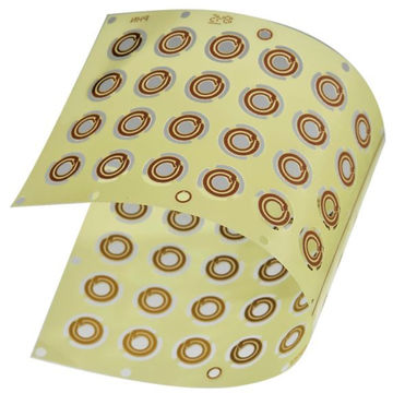
Die dünnsten Leiterplatten (Leiterplatten) stellen einen bedeutenden Fortschritt im elektronischen Design dar, Ermöglicht ultraschlanke und leichte Geräte ohne Kompromisse bei der Funktionalität. Diese Leiterplatten sind unverzichtbar bei Anwendungen, bei denen Platz und Gewicht entscheidende Faktoren sind. Dieser Artikel befasst sich mit den Eigenschaften, Struktur, Materialien, Herstellungsprozesse, Anwendungen, Vorteile, und häufig gestellte Fragen (FAQs) bezogen auf die dünnsten Leiterplatten.
Struktur der dünnsten Leiterplatten
Die Struktur der dünnsten Leiterplatten wurde sorgfältig entwickelt, um die Leistung aufrechtzuerhalten und gleichzeitig die Dicke zu reduzieren:
In der Regel aus Hochleistungsmaterial hergestellt, flexible Materialien wie Polyimid oder ultradünnes FR-4 sorgen für mechanische Stabilität und Flexibilität.
Extrem dünne Kupferschichten, manchmal so dünn wie 9 Mikrometer (μm), werden für Leiterbahnen verwendet.
Ultradünne dielektrische Materialien zwischen leitfähigen Schichten sorgen für elektrische Isolierung ohne zusätzliche Masse.
Spezialklebstoffe, die dünn, aber stark sind, um die Schichten sicher zu verbinden.
Gewährleistet die Lötbarkeit und schützt freiliegendes Kupfer vor Oxidation.
Materialien, die in den dünnsten Leiterplatten verwendet werden
Zu den wichtigsten Materialien, die in den dünnsten Leiterplatten verwendet werden, gehören::
Ein flexibles und hitzebeständiges Material, das sich aufgrund seiner Haltbarkeit und Hochleistungseigenschaften ideal für dünne Leiterplatten eignet.
Eine dünne Version des Standard-FR-4-Laminats, das in herkömmlichen Leiterplatten verwendet wird, bietet gute mechanische Festigkeit und elektrische Isolierung.
Zur Herstellung von Leiterbahnen werden dünne Kupferfolien bei minimaler Dicke verwendet.
Materialien wie Flüssigkristallpolymer (LCP) oder Teflon (PTFE) werden wegen ihrer hervorragenden elektrischen Eigenschaften und minimalen Dicke verwendet.
Dünn, Hochleistungsklebstoffe, die Integrität und Festigkeit bewahren, ohne nennenswertes Volumen hinzuzufügen.
Herstellungsprozess der dünnsten Leiterplatten
Der Herstellungsprozess für die dünnsten Leiterplatten umfasst mehrere präzise Schritte, um Qualität und Zuverlässigkeit sicherzustellen:
Auswahl und Vorbereitung ultradünner Basismaterialien, Kupferfolien, und Dielektrika.
Die Schichten werden unter hohem Druck und hoher Temperatur mit speziellen dünnen Klebstoffen zusammenlaminiert.
Zur Strukturierung der Kupferschichten wird Fotolithographie eingesetzt, Definieren der Schaltungspfade.
Durch chemisches Ätzen wird überschüssiges Kupfer entfernt, hinterlässt die gewünschten Schaltungsmuster.
Beim Präzisionsbohren entstehen Durchkontaktierungen und Löcher für Zwischenschichtverbindungen und Komponentenmontage.
Durch Galvanisieren wird den Durchkontaktierungen Kupfer hinzugefügt, Verbesserung der elektrischen Konnektivität.
Aufbringen von Oberflächenveredelungen wie ENIG (Chemisches Nickel-Immersionsgold) um das Kupfer zu schützen und die Lötbarkeit sicherzustellen.
Strenge Inspektionen und elektrische Tests stellen sicher, dass die Leiterplatte den Designspezifikationen und Leistungsstandards entspricht.
Anwendungen der dünnsten Leiterplatten
Die dünnsten Leiterplatten werden in einer Vielzahl von High-Tech-Anwendungen eingesetzt:
Smartphones, Tabletten, und tragbare Geräte, bei denen der Platz knapp ist.
Implantierbare Geräte und tragbare medizinische Geräte, die eine minimale Größe und ein minimales Gewicht erfordern.
Kompakt, Leichtbauelektronik für Satelliten, Drohnen, und militärische Ausrüstung.
Fortschrittliche Fahrerassistenzsysteme (Adas) und Infotainmentsysteme in Fahrzeugen.
Hochfrequenzgeräte und kompakte Kommunikationsmodule.
Vorteile der dünnsten Leiterplatten
Die dünnsten Leiterplatten bieten mehrere wesentliche Vorteile:
Ermöglicht das Design ultrakompakter und leichter elektronischer Geräte.
Besonders wenn es aus Materialien wie Polyimid besteht, Sie können ohne Beschädigung gebogen und gefaltet werden, nützlich in flexibler Elektronik.
Trotz ihrer Dünnheit, Sie gewährleisten eine hervorragende elektrische Leistung und Signalintegrität.
Effiziente Wärmeableitung trotz kompaktem Formfaktor.
Geeignet für ein breites Anwendungsspektrum in verschiedenen Branchen.
FAQ
Was sind die größten Herausforderungen bei der Herstellung dünnster Leiterplatten??
Die Herstellung dünnster Leiterplatten bringt Herausforderungen mit sich, wie zum Beispiel die beschädigungsfreie Handhabung ultradünner Materialien, Aufrechterhaltung einer präzisen Ausrichtung während der Laminierung, und Gewährleistung zuverlässiger elektrischer Verbindungen bei minimaler Materialstärke.
Wie schneiden die dünnsten Leiterplatten im Hinblick auf die Leistung im Vergleich zu herkömmlichen Leiterplatten ab??
Die dünnsten Leiterplatten können in vielerlei Hinsicht mit der Leistung herkömmlicher Leiterplatten mithalten oder diese sogar übertreffen, einschließlich elektrischer Leistung und Wärmemanagement, dank fortschrittlicher Materialien und präziser Herstellungsverfahren.
Welche Branchen profitieren am meisten vom Einsatz dünnster Leiterplatten??
Branchen wie Unterhaltungselektronik, Medizinprodukte, Luft- und Raumfahrt, Automobil, und Telekommunikation profitieren aufgrund ihrer platzsparenden und leistungsstarken Eigenschaften erheblich vom Einsatz dünnster Leiterplatten.
Wie gewährleisten die dünnsten Leiterplatten trotz ihrer geringen Dicke Zuverlässigkeit??
Die dünnsten Leiterplatten gewährleisten Zuverlässigkeit durch die Verwendung hochwertiger Materialien, Präzise Herstellungsprozesse, und strenge Tests, um strenge Leistungs- und Haltbarkeitsstandards zu erfüllen.