CO.,LTD")
Hersteller von Ultra-Multilayer-FC-LGA-Substraten. Als führender Hersteller von Ultra-Multilayer-FC-LGA-Substraten, Wir sind darauf spezialisiert, Höchstleistungen zu erbringen, zuverlässige Verbindungslösungen für fortschrittliche elektronische Anwendungen. Unsere hochmodernen Herstellungsprozesse und strengen Qualitätskontrollen gewährleisten eine hervorragende Signalintegrität, Wärmemanagement, und Miniaturisierung. Ideal für hohe Dichte, High-Speed-Computing-Umgebungen, Unsere Substrate unterstützen Spitzentechnologien wie 5G, KI, und Rechenzentren, Wir ermöglichen unseren Kunden, beispiellose Leistung und Innovation bei ihren Produkten zu erzielen.
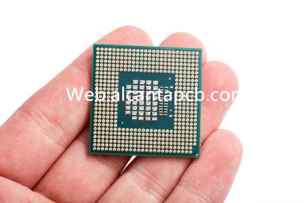
Ultra-Multilayer-Flip-Chip-Land-Grid-Array (FC-LGA) Substrate sind entscheidende Komponenten bei der Verpackung von Hochleistungshalbleiterbauelementen. Diese fortschrittlichen Substrate unterstützen die steigenden Anforderungen an höhere Leistung, Miniaturisierung, und Wärmemanagement in modernen elektronischen Geräten. In diesem Artikel werden die Merkmale untersucht, Konstruktionsüberlegungen, Materialien, Herstellungsprozesse, Anwendungen, und Vorteile von Ultra-Multilayer FC-LGA Substrate.
Was sind Ultra-Multilayer-FC-LGA-Substrate??
Ultra-Multilayer-FC-LGA-Substrate sind spezielle Verpackungssubstrate, die in der Flip-Chip-Technologie verwendet werden, wo integrierte Schaltkreise (ICs) werden mit der Vorderseite nach unten auf dem Substrat mithilfe von Löthöckern für direkte elektrische Verbindungen montiert. Das Land Grid Array (LGA) Das Format bietet ein Kontaktraster auf der Unterseite des Substrats, Dies ermöglicht zuverlässige und effiziente elektrische Verbindungen. Diese Substrate sind mit mehreren Schichten ausgelegt, um Verbindungen mit hoher Dichte und erweitertes Routing zu ermöglichen, Dadurch sind sie für Hochleistungsanwendungen geeignet.
Designüberlegungen für Ultra-Multilayer-FC-LGA-Substrate
Das Entwerfen von Ultra-Multilayer-FC-LGA-Substraten erfordert mehrere wichtige Überlegungen:
Auswahl der richtigen Materialien mit geeigneten dielektrischen Eigenschaften, Wärmeleitfähigkeit, und die mechanische Festigkeit ist entscheidend für eine optimale Leistung.
Um eine Überhitzung zu verhindern und einen zuverlässigen Betrieb zu gewährleisten, ist ein effizientes Wärmemanagement unerlässlich. Dazu gehört auch die Einbindung thermischer Vias, Wärmespreizner, und andere Kühlmechanismen.
3. **Signalintegrität:** Die Aufrechterhaltung der Signalintegrität bei hohen Frequenzen erfordert eine sorgfältige Kontrolle der Spurenimpedanz, Minimierung des Übersprechens, und Implementierung wirksamer Erdungs- und Abschirmtechniken.
Der Untergrund muss über ausreichende mechanische Festigkeit und Stabilität verfügen, um Herstellungsprozessen und Betriebsbedingungen standzuhalten, einschließlich thermischer Zyklen und mechanischer Beanspruchung.
Die Oberflächenbeschaffenheit muss glatt und fehlerfrei sein, um eine ordnungsgemäße Haftung und Ausrichtung der Komponenten zu gewährleisten und Signalverluste und Reflexionen zu minimieren.
Materialien, die in Ultra-Multilayer-FC-LGA-Substraten verwendet werden
Bei der Herstellung von Ultra-Multilayer-FC-LGA-Substraten werden üblicherweise mehrere Materialien verwendet:
Materialien wie Aluminiumoxid (AL2O3), Aluminiumnitrid (AlN), und Berylliumoxid (BeO) bieten hervorragende dielektrische Eigenschaften und eine hohe Wärmeleitfähigkeit.
Hochfrequenzlaminate, wie PTFE (Polytetrafluorethylen) und keramisch gefüllte PTFE-Verbundwerkstoffe, sorgen für niedrige Dielektrizitätskonstanten und Verlustfaktorwerte, Gewährleistung minimaler Signalverluste.
Aufgrund ihrer hervorragenden elektrischen Leitfähigkeit und Zuverlässigkeit werden Kupfer und andere Metalllegierungen für Leiterbahnen und Durchkontaktierungen verwendet.
Als Klebematerialien werden Hochleistungs-Epoxidharze eingesetzt, um die Schichten des Untergrundes miteinander zu verbinden, Bereitstellung mechanischer Stärke und Stabilität.
Diese werden auf die Kontaktpads angewendet, um die Lötlichkeit zu verbessern und vor Oxidation zu schützen.
Herstellungsprozess von Ultra-Multilayer-FC-LGA-Substraten
Der Herstellungsprozess von Ultra-Multilayer-FC-LGA-Substraten umfasst mehrere präzise Schritte:
Die Rohstoffe, einschließlich Hochleistungskeramik, organische Laminate, und Metalllegierungen, werden zu Blättern oder Filmen vorbereitet und verarbeitet.
Mehrere Schichten des Substratmaterials werden zusammen laminiert, um eine Aufbaustruktur zu bilden. Bei diesem Vorgang werden Wärme und Druck angewendet, um die Schichten zu verbinden.
Schaltungsmuster werden unter Verwendung photolithographischer Prozesse erzeugt. Ein photosensitiver Film (Fotolack) wird auf das Substrat angewendet, Ultraviolett ausgesetzt (UV) Licht durch eine Maske, und entwickelt, um die gewünschten Schaltungsmuster aufzudecken. Das Substrat wird dann geätzt, um unerwünschtes Material zu entfernen.
VIAS werden in das Substrat gebohrt, um vertikale elektrische Verbindungen zwischen verschiedenen Schichten herzustellen. Diese Löcher werden dann mit Kupfer plattiert, um leitende Pfade herzustellen.
Eine glatte, Auf die Kontaktpads wird eine fehlerfreie Oberflächenveredelung aufgetragen, um eine ordnungsgemäße Haftung und Ausrichtung der Komponenten sicherzustellen, sowie zur Minimierung von Signalverlust und Reflexion.
Die fertigen Substrate werden strengen Tests und Inspektionen unterzogen, um sicherzustellen, dass sie die erforderlichen Spezifikationen für die elektrische Leistung erfüllen, Signalintegrität, und Zuverlässigkeit.
Anwendungen von Ultra-Multilayer-FC-LGA-Substraten
Ultra-Multilayer-FC-LGA-Substrate werden in einer Vielzahl von Hochleistungsanwendungen eingesetzt:
Diese Substrate werden in Hochleistungsprozessoren und Mikrocontrollern eingesetzt, Bereitstellung der notwendigen elektrischen und thermischen Eigenschaften für einen zuverlässigen Betrieb.
Ultra-Multilayer-FC-LGA-Substrate werden in Speichergeräten verwendet, einschließlich DRAM und Flash-Speicher, wo hochdichte Verbindungen und Signalintegrität von entscheidender Bedeutung sind.
Diese Substrate unterstützen fortschrittliche Kommunikationssysteme, einschließlich 5G -Basisstationen und Netzwerkinfrastruktur, wo Hochgeschwindigkeitsbetrieb und Signalintegrität unerlässlich sind.
Ultra-Multilayer-FC-LGA-Substrate werden in der Unterhaltungselektronik eingesetzt, wie Smartphones, Tabletten, und tragbare Geräte, wo Miniaturisierung und Leistung entscheidend sind.
Die Substrate werden in der Automobilelektronik eingesetzt, einschließlich fortschrittlicher Fahrerassistenzsysteme (Adas) und Infotainmentsysteme, erfordern robuste Leistung und Zuverlässigkeit.
Vorteile von Ultra-Multilayer-FC-LGA-Substraten
Ultra-Multilayer-FC-LGA-Substrate bieten mehrere Vorteile:
Das mehrschichtige Design ermöglicht Verbindungen mit hoher Dichte, Dies ermöglicht komplexes Routing und erhöhte Funktionalität.
Diese Substrate bieten eine hervorragende elektrische Leistung, einschließlich geringem Signalverlust und hoher Signalintegrität, entscheidend für Hochgeschwindigkeitsanwendungen.
Materialien mit hoher Wärmeleitfähigkeit sorgen für eine effiziente Wärmeableitung, Vermeidung von Überhitzung und Gewährleistung eines zuverlässigen Betriebs.
Die Substrate bieten eine robuste mechanische Unterstützung, Gewährleistung der Zuverlässigkeit und Haltbarkeit der verpackten Komponenten unter verschiedenen Umgebungsbedingungen.
Die Fähigkeit, feine Strukturen und hochdichte Verbindungen zu schaffen, unterstützt die Miniaturisierung von Halbleitergehäusen, Dadurch sind sie für kompakte elektronische Geräte geeignet.
FAQ
Was sind die Hauptvorteile der Verwendung von Ultra-Multilayer-FC-LGA-Substraten??
Zu den Hauptvorteilen gehören Verbindungen mit hoher Dichte, Überlegene elektrische Leistung, effizientes Thermomanagement, mechanische Stabilität, und Unterstützung der Miniaturisierung. Diese Substrate bilden die Grundlage für die Herstellung leistungsstarker Halbleiterbauelemente.
Welche Materialien werden üblicherweise in Ultra-Multilayer-FC-LGA-Substraten verwendet??
Zu den gängigen Materialien gehört Hochleistungskeramik (wie Aluminiumoxid, Aluminiumnitrid, und Berylliumoxid), organische Laminate (wie PTFE und keramisch gefüllte PTFE-Verbundwerkstoffe), Metalllegierungen (wie Kupfer), Epoxidharze, und Nickel/Gold -Oberflächen.
Wie gewährleistet das Design eines Ultra-Multilayer-FC-LGA-Substrats die Signalintegrität??
Das Design gewährleistet die Signalintegrität durch niedrige Werte für Dielektrizitätskonstante und Verlustfaktor, Kontrolle der Spurenimpedanz, Minimierung des Übersprechens, und Implementierung wirksamer Erdungs- und Abschirmtechniken. Simulationstools werden verwendet, um diese Aspekte für die Hochfrequenzleistung zu optimieren.
Was sind die häufigsten Anwendungen von Ultra-Multilayer-FC-LGA-Substraten??
Zu den gängigen Anwendungen gehören Prozessoren und Mikrocontroller, Speichergeräte, fortgeschrittene Kommunikationssysteme, Unterhaltungselektronik, und Automobilelektronik. Diese Substrate werden in Systemen verwendet, die hochdichte Verbindungen erfordern, Überlegene elektrische Leistung, und effizientes Wärmemanagement.