CO.,LTD")
Hersteller ultradünner CPU-BGA-Substrate.”Hersteller ultradünner CPU-BGA-Substrate” bezieht sich auf ein Unternehmen, das sich auf die Herstellung ultradünner Ball Grid Arrays spezialisiert hat (BGA) Substrate für CPUs. Sie konzentrieren sich darauf, dünn zu werden, hochdichte Verbindungslösungen, die die Leistung und Effizienz elektronischer Geräte verbessern.
In moderner elektronischer Technologie, Ultradünne CPU BGA-Substrate sind eine der Schlüsselkomponenten. Sie zeichnen sich nicht nur durch Leistung und Größe aus, Sie fördern auch die Miniaturisierung und Hocheffizienz elektronischer Geräte. In diesem Artikel werden verschiedene Aspekte dieser Substrate im Detail untersucht.
Was sind ultradünne CPU-BGA-Substrate??
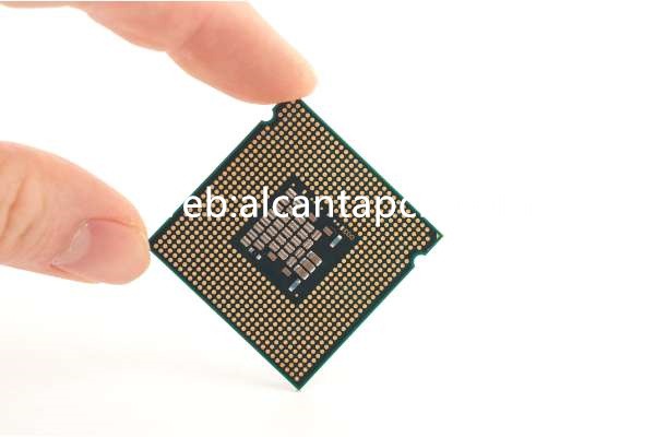
Ultradünne CPU-BGA Substrate siehe ultradünnes Ball-Grid-Array (BGA) Substrate, die zur Verbindung und Unterstützung der Zentraleinheit verwendet werden (CPU) und andere elektronische Komponenten. Dieses Substrat trägt nicht nur die CPU, sondern sorgt auch für die Signalübertragung und Stromverteilung durch hochentwickelte Schaltkreise und Verkabelungen. Sein Hauptmerkmal ist seine extrem geringe Dicke, normalerweise zwischen einigen hundert Mikrometern und einigen Millimetern.
Diese Substrate spielen in modernen elektronischen Geräten eine entscheidende Rolle. Da die Anforderungen an die Geräteleistung steigen und die Größe abnimmt, Substrate mit herkömmlichen Dicken können den Anforderungen an hohe Dichte und Leistung nicht mehr gerecht werden. Ultradünne Substrate können eine höhere elektrische Leistung und Wärmeableitungseffizienz bieten, indem sie die Dicke reduzieren und Materialien und Design optimieren.
Beim Design ultradünner CPU-BGA-Substrate müssen mehrere Faktoren berücksichtigt werden. Die erste ist die Materialauswahl, Dabei werden üblicherweise hochdichte organische Harze verwendet, Keramik und Metallwerkstoffe. Diese Materialien müssen nicht nur eine gute elektrische Leitfähigkeit aufweisen, sondern auch in Hochtemperaturumgebungen stabil arbeiten können. Der zweite Faktor ist die mechanische Festigkeit und Haltbarkeit. Ein ultradünnes Design ist erforderlich, um sicherzustellen, dass das Substrat im Langzeitgebrauch nicht aufgrund mechanischer Belastungen versagt. Zusätzlich, Auch die elektrische Leistung ist entscheidend, und Designer müssen sicherstellen, dass das Substrat einen Pfad mit geringem Widerstand und hoher Leitfähigkeit bieten kann, um die Stabilität und Zuverlässigkeit der Signalübertragung sicherzustellen.
In praktischen Anwendungen, Ultradünne CPU-BGA-Substrate verbessern nicht nur die Leistung des Geräts, sondern reduzieren auch die Größe und das Gewicht des Geräts erheblich. Dies ist besonders wichtig für tragbare Geräte wie Smartphones, Tabletten, und Laptops. Für diese Geräte gelten strenge Anforderungen an Tragbarkeit und Akkulaufzeit, und ultradünne Substrate erfüllen diese Anforderungen durch ihre hervorragende Leistung und ihr Design.
Auch im Hochleistungsrechnen weisen ultradünne Substrate großes Potenzial auf. Geräte wie Server, Rechenzentren, und Beschleuniger für künstliche Intelligenz müssen große Datenmengen und komplexe Rechenaufgaben verarbeiten, und stellen extrem hohe Anforderungen an die elektrische Leistung und die Wärmeableitungsfähigkeiten des Substrats. Ultradünne CPU-BGA-Substrate können durch ihre hohe Leitfähigkeit und hohe Wärmeableitung die Effizienz und Zuverlässigkeit dieser Geräte effektiv verbessern.
Zusätzlich, Auch die Herstellung ultradünner Substrate schreitet voran. Fortschrittliche Fertigungsprozesse und -technologien machen die Produktion ultradünner Substrate präziser und effizienter. Zum Beispiel, Laserschneid- und Mikrobearbeitungstechnologien können eine extrem hohe Fertigungspräzision erreichen und die Konsistenz und Stabilität der Mikrostruktur des Substrats gewährleisten. Gleichzeitig, Die Einführung automatisierter Produktionslinien hat die Produktionseffizienz und den Ertrag erheblich verbessert, reduzierte Produktionskosten, und ermöglichte den Einsatz ultradünner Substrate in mehr Bereichen.
Im Allgemeinen, Ultradünne CPU-BGA-Substrate sind ein wichtiger Treiber für die Entwicklung moderner elektronischer Technologie. Durch ihr einzigartiges Design und ihre hervorragende Leistung, Diese Substrate verbessern nicht nur die Gesamtleistung des Geräts, sondern fördern auch die Miniaturisierung und hohe Leistung elektronischer Geräte. Mit der kontinuierlichen Weiterentwicklung und Innovation der Technologie, Ultradünne Substrate werden in Zukunft breitere Einsatzmöglichkeiten und eine höhere Leistung bieten.
Design-Referenzhandbuch für ultradünne CPU-BGA-Substrate
Entwicklung ultradünner CPU-BGA-Substrate (ultradünne CPU-BGA-Substrate) ist eine komplexe und heikle Aufgabe, die die Einhaltung einer Reihe strenger Designrichtlinien und -standards erfordert. Diese Richtlinien betreffen nicht nur die Materialauswahl, mechanisches Design, elektrisches Design, usw., sondern auch Produktionsprozesse betreffen, Prüfung und Qualitätskontrolle. Nachfolgend finden Sie einige wichtige Referenzrichtlinien für die Entwicklung ultradünner CPU-BGA-Substrate.
Erstens, Die Materialauswahl ist die Grundlage des Designs. Ultradünne CPU-BGA-Substrate verwenden normalerweise hochdichte organische Harze (wie FR-4), Keramik und Metallwerkstoffe. FR-4 wird aufgrund seiner guten mechanischen Eigenschaften und elektrischen Isolationseigenschaften häufig verwendet. Keramische Materialien, zeichnen sich durch eine hervorragende Wärmeleitfähigkeit und hohe Temperaturstabilität aus, eignen sich für Anwendungen mit hoher Leistung und hohen Anforderungen an die Wärmeableitung. Zusätzlich, um die Leitfähigkeit des Substrats zu verbessern, Normalerweise wird eine Schicht aus Kupfer oder anderen leitfähigen Materialien auf und innerhalb des Substrats plattiert.
Zweitens, Die Dicke und Anzahl der Schichten des Substrats müssen basierend auf den spezifischen Anwendungsanforderungen optimiert werden. Der Schlüssel zum ultradünnen Design liegt darin, den optimalen Kompromiss zwischen Leistung und Kosten zu finden. Ein zu dünner Untergrund kann zu einer unzureichenden mechanischen Festigkeit führen, während ein zu dickes Substrat die Anforderungen der Miniaturisierung und der Integration hoher Dichte nicht erfüllen kann. Designer müssen durch genaue Berechnungen und Simulationen die am besten geeignete Dicke und Anzahl der Schichten bestimmen.
In Bezug auf Layout und Verkabelungsdesign, Ein vernünftiges Layout kann Signalstörungen reduzieren und die Gesamtleistung des Systems verbessern. Designer müssen sicherstellen, dass die Signalpfadlängen auf ein Minimum beschränkt werden und unnötige Biegungen und Überkreuzungen vermieden werden. Zusätzlich, Auch die Gestaltung der Stromversorgung und der Erdungskabel muss berücksichtigt werden, um die Stabilität der Stromversorgung und die Entstörungsfähigkeit des Systems sicherzustellen. Zur Hochfrequenzsignalverarbeitung, Designer müssen der Impedanzanpassung und dem Abschirmungsdesign von Leiterbahnen besondere Aufmerksamkeit widmen, um Signalreflexion und Strahlungsverluste zu reduzieren.
Um die Genauigkeit und Zuverlässigkeit von Designs sicherzustellen, Designer verwenden in der Regel fortschrittliche Designtools und Simulationssoftware. Diese Werkzeuge können das Verhalten von Substraten unter verschiedenen Betriebsbedingungen simulieren, Unterstützung von Designern bei der Identifizierung und Lösung potenzieller Probleme. Zum Beispiel, Eine elektromagnetische Simulationssoftware kann die Übertragung von Signalen auf einem Substrat simulieren und mögliche Störungen und Verluste analysieren. Wärmesimulationssoftware kann die Wärmeverteilung des Substrats simulieren und Designer dabei unterstützen, das Wärmeableitungsdesign zu optimieren.
Nachdem der Entwurf abgeschlossen ist, Es sind eine Reihe von Tests und Überprüfungen erforderlich, um sicherzustellen, dass die tatsächliche Leistung des Substrats den Designanforderungen entspricht. Zu den gängigen Testmethoden gehört die Prüfung der elektrischen Leistung, mechanische Festigkeitsprüfung, Thermozyklusprüfung, usw. Diese Tests können potenzielle Probleme mit dem Substrat im tatsächlichen Gebrauch identifizieren und sicherstellen, dass es unter verschiedenen Betriebsbedingungen stabil funktionieren kann.
Endlich, Auch die Qualitätskontrolle ist ein wichtiger Teil des Designprozesses. Eine strenge Qualitätskontrolle gewährleistet die Leistung und Zuverlässigkeit jedes Substrats. Designer müssen detaillierte Qualitätskontrollstandards und -prozesse entwickeln, inklusive Materialprüfung, Kontrolle des Produktionsprozesses, Inspektion des fertigen Produkts, usw. Durch umfassende Qualitätskontrolle, Die Produktionsfehlerrate kann erheblich reduziert und die Gesamtqualität des Produkts verbessert werden.
Zusamenfassend, Das Entwerfen ultradünner CPU-BGA-Substrate ist eine komplexe Aufgabe, die eine umfassende Berücksichtigung mehrerer Faktoren erfordert. Von der Materialauswahl, vom mechanischen Design bis zur elektrischen Leistung und dem Wärmemanagement, Jeder Link erfordert sorgfältiges Design und strenge Kontrolle. Durch Befolgen einer Reihe von Designrichtlinien und -standards, Designer können ultradünne Substrate mit hervorragender Leistung und hoher Zuverlässigkeit entwickeln, starke Unterstützung für die Entwicklung moderner elektronischer Geräte.
Welches Material wird in ultradünnen CPU-BGA-Substraten verwendet??
Ultradünne CPU-BGA-Substrate verwenden eine Vielzahl von Hochleistungsmaterialien. Die Auswahl und Anwendung dieser Materialien hat einen entscheidenden Einfluss auf die Leistung, Zuverlässigkeit und Herstellungsprozess des Substrats. Im Folgenden sind einige häufig verwendete Materialien und ihre Anwendungen und Eigenschaften in ultradünnen CPU-BGA-Substraten aufgeführt.
Erstens, Organische Harzmaterialien wie FR-4 sind die am häufigsten verwendeten Substratmaterialien. FR-4 ist ein glasfaserverstärktes Epoxidharzmaterial mit hervorragender mechanischer Festigkeit und elektrischen Isolationseigenschaften. Es ist nicht nur beständig gegen Hitze und chemische Korrosion, sondern sorgt auch für eine stabile elektrische Leistung, Daher wird es häufig bei der Substratherstellung verschiedener elektronischer Produkte verwendet. Für ultradünne CPU-BGA-Substrate, FR-4 kann durch eine verbesserte Formulierung und einen verbesserten Prozess die Dicke weiter reduzieren und gleichzeitig seine mechanische und elektrische Leistung beibehalten.
Keramikmaterialien sind auch eine wichtige Wahl bei ultradünnen CPU-BGA-Substraten. Zu den häufig verwendeten Keramikmaterialien gehört Aluminiumoxid (AL2O3) und Aluminiumnitrid (AlN). Diese Materialien verfügen über eine extrem hohe Wärmeleitfähigkeit und elektrische Isolationseigenschaften, und kann in Hochtemperaturumgebungen stabil arbeiten. Aluminiumoxid hat gute mechanische Eigenschaften und ist kostengünstig, während Aluminiumnitrid aufgrund seiner höheren Wärmeleitfähigkeit und elektrischen Eigenschaften für anspruchsvollere Anwendungen geeignet ist. Bei der Gestaltung ultradünner Substrate, Keramikmaterialien können die Wärmeableitungskapazität des Substrats effektiv verbessern und den stabilen Betrieb der CPU gewährleisten.
Metallmaterialien, wie Kupfer und Kupferlegierungen, werden hauptsächlich für leitfähige Schichten und Wärmeableitungsschichten in ultradünnen CPU-BGA-Substraten verwendet. Kupfer verfügt über eine hervorragende elektrische und thermische Leitfähigkeit und kann elektrische Signale effektiv leiten und Wärme ableiten. In der Substratherstellung, Galvanisierungs- und Ätzverfahren werden häufig verwendet, um präzise leitfähige Muster auf und innerhalb des Substrats zu bilden. Für Hochleistungsanwendungen, Kupferlegierungen können auch verwendet werden, um die mechanische Festigkeit und Ermüdungsbeständigkeit von Kupfer durch die Einführung von Legierungselementen zu verbessern.
In den letzten Jahren, Neue Materialien wie Graphen werden auch zunehmend in ultradünnen CPU-BGA-Substraten eingesetzt. Graphen ist ein zweidimensionales Material, das aus einer einzigen Schicht von Kohlenstoffatomen besteht und eine extrem hohe elektrische Leitfähigkeit aufweist, Wärmeleitfähigkeit und mechanische Festigkeit. Seine einzigartigen physikalischen und chemischen Eigenschaften verleihen Graphen ein großes Anwendungspotenzial in ultradünnen Substraten. Zum Beispiel, durch Zugabe von Graphen zum Substratmaterial, Die Wärmeleitfähigkeit und die elektrische Leistung des Substrats können deutlich verbessert werden, die Dicke kann reduziert werden, und die mechanische Festigkeit kann verbessert werden.
Zusätzlich, um die Leistung und Zuverlässigkeit des Substrats weiter zu verbessern, Designer werden eine Vielzahl von Verbundmaterialien und -strukturen verwenden. Zum Beispiel, durch Vermischen eines organischen Harzmaterials mit einem Keramikpulver, Es kann ein Substrat erhalten werden, das sowohl die Flexibilität des organischen Materials als auch die hohe Wärmeleitfähigkeit des Keramikmaterials aufweist. Ähnlich, durch mehrschichtiges Strukturdesign, Die Vorteile verschiedener Materialien können in das Substrat integriert werden, wie zum Beispiel die Verwendung hochleitfähiger Materialien in der Außenschicht und hochfester Materialien in der Mittelschicht, Dadurch wird die beste Leistungsbalance erreicht.
Bei der Auswahl und Anwendung dieser Materialien, Es müssen mehrere Faktoren berücksichtigt werden, einschließlich der mechanischen Eigenschaften des Materials, elektrische Eigenschaften, Wärmeleitfähigkeit, kosten, und Verarbeitungstechniken. Zum Beispiel, für Anwendungen, die eine hohe Wärmeleitfähigkeit und Zuverlässigkeit erfordern, wie Hochleistungsrechnen und Rechenzentren, Hochleistungsmaterialien wie Keramik und Graphen können bevorzugt werden. Für Unterhaltungselektronik, Sie können Kosten und Verarbeitbarkeit stärker berücksichtigen und optimierte organische Harzmaterialien wählen.
Gesamt, Die Materialauswahl für ultradünne CPU-BGA-Substrate ist ein komplexer und kritischer Prozess. Durch die rationale Auswahl und Kombination verschiedener Hochleistungsmaterialien, Das Substrat kann hinsichtlich der mechanischen Festigkeit die beste Leistung erzielen, elektrische Leistung, und Wärmemanagement, Dadurch werden die Anforderungen verschiedener elektronischer High-End-Geräte erfüllt.
Welche Größe haben ultradünne CPU-BGA-Substrate??
Die Größe und Form ultradünner CPU-BGA-Substrate (ultradünne CPU-BGA-Substrate) variieren je nach Anwendungsanforderungen. Die Dicke, Länge und Breite dieser Substrate müssen entsprechend dem spezifischen CPU-Paket und der Anwendungsumgebung angepasst werden. Im Folgenden finden Sie eine detaillierte Diskussion des Größendesigns von ultradünnen CPU-BGA-Substraten.
Erste, Die Dicke des Substrats ist ein kritischer Parameter. Typischerweise, Die Dicke ultradünner CPU-BGA-Substrate reicht von einigen hundert Mikrometern bis zu einigen Millimetern. Die konkrete Dickenauswahl hängt von verschiedenen Faktoren ab, einschließlich mechanischer Festigkeit, elektrische Eigenschaften und Wärmeableitungsfähigkeiten. Für tragbare Geräte, wie Smartphones und Tablets, Designer neigen oft dazu, möglichst dünne Substrate zu wählen, um die Gesamtgröße und das Gewicht des Geräts zu reduzieren. Jedoch, Ein zu dünner Untergrund kann zu unzureichender mechanischer Festigkeit führen und sich während des Gebrauchs leicht verbiegen oder brechen. daher, während des Designprozesses, Es ist notwendig, durch genaue Berechnung und Simulation den besten Gleichgewichtspunkt zwischen Dicke und Festigkeit zu finden.
Anschließend wird die Dicke des Untergrundes bestimmt, Auch die Länge und Breite des Untergrundes müssen entsprechend der konkreten Anwendung ausgelegt werden. Unterschiedliche CPU-Paketgrößen und Layoutanforderungen wirken sich auf die Gesamtabmessungen des Substrats aus. Allgemein gesprochen, Die Länge und Breite des Substrats sollte in der Lage sein, das CPU-Paket und andere notwendige elektronische Komponenten vollständig abzudecken, und reservieren Sie ausreichend Platz für die Signalverkabelung und Stromverteilung. Zusätzlich, Die Form des Substrats muss außerdem zum äußeren Design des Geräts passen, um beim Zusammenbau einen festen Sitz mit anderen Komponenten zu gewährleisten.
Um die Designflexibilität und Anpassungsfähigkeit zu verbessern, Das Größendesign ultradünner CPU-BGA-Substrate folgt normalerweise einem modularen und maßgeschneiderten Ansatz. Der modulare Aufbau ermöglicht Designern die Auswahl und Kombination von Baseboard-Modulen unterschiedlicher Größe und Form entsprechend den unterschiedlichen Anwendungsanforderungen, um optimale Leistung und Kosteneffizienz zu erzielen. Das maßgeschneiderte Design basiert auf den besonderen Anforderungen spezifischer Projekte, mit speziellen Größen- und Layoutdesigns, um den Anforderungen spezifischer Anwendungen gerecht zu werden.
Auch die Verdrahtungsdichte ist ein wichtiger Aspekt bei der Dimensionierung. Da die Funktionalität elektronischer Geräte immer weiter zunimmt, Dies gilt auch für die Anzahl der elektronischen Komponenten und Verbindungspunkte auf dem Substrat. Entwickler müssen diese Komponenten und Verbindungspunkte sinnvoll auf einer begrenzten Substratfläche anordnen, um die Stabilität der Signalübertragung und die Zuverlässigkeit der Stromverteilung sicherzustellen. Zu diesem Zweck, Um die Verdrahtungsdichte und die Integration des Substrats durch Optimierung der Verdrahtungspfade und Zwischenschichtverbindungen zu verbessern, müssen fortschrittliche Verdrahtungstechnologie und Designtools eingesetzt werden.
Zusätzlich, Bei der Größengestaltung des Substrats müssen auch der Produktionsprozess und die Kosten berücksichtigt werden. Ein zu komplexes und präzises Maßdesign kann die Produktionsschwierigkeiten und -kosten erhöhen, Auswirkungen auf die Wirtschaftlichkeit des Endprodukts haben. Designer müssen durch Prozessoptimierung und Kostenkontrolle das beste Gleichgewicht zwischen Leistung und Kosten finden. Zum Beispiel, während des Designprozesses, Standardisierte Größen und Vorlagen können verwendet werden, um Komplexität und Variabilität im Produktionsprozess zu reduzieren und die Produktionseffizienz und -ausbeute zu verbessern.
In tatsächlichen Anwendungen, Das Größendesign ultradünner CPU-BGA-Substrate erfordert noch eine Reihe von Tests und Überprüfungen. Durch die Herstellung und Prüfung physischer Muster, die Machbarkeit und Zuverlässigkeit des Entwurfs kann überprüft werden, und potenzielle Probleme können entdeckt und gelöst werden. Zu den gängigen Prüfmethoden gehört die Prüfung der mechanischen Festigkeit, elektrische Leistungsprüfung, Thermozyklusprüfung, usw. Diese Tests können die Leistung und Zuverlässigkeit des Substrats im tatsächlichen Einsatz sicherstellen und den Anforderungen verschiedener Betriebsbedingungen gerecht werden.
Im Allgemeinen, Das Größendesign von ultradünnen CPU-BGA-Substraten ist ein komplexer und kritischer Prozess, der eine umfassende Berücksichtigung mehrerer Faktoren wie der mechanischen Leistung erfordert, elektrische Leistung, Wärmeableitungskapazität, Produktionsprozess und Kosten. Durch angemessenes Größendesign, Das optimale Gleichgewicht zwischen Leistung und Wirtschaftlichkeit des Substrats kann erreicht werden, um den Anforderungen verschiedener elektronischer High-End-Geräte gerecht zu werden.
Der Herstellungsprozess ultradünner CPU-BGA-Substrate
Der Herstellungsprozess von ultradünnen CPU-BGA-Substraten (ultradünnes CPU-BGA-Substrat) ist komplex und präzise und erfordert mehrere Prozesse. Jeder Prozess erfordert eine strenge Kontrolle und Optimierung, um die Qualität und Leistung des Endprodukts sicherzustellen. Im Folgenden finden Sie eine detaillierte Beschreibung des Herstellungsprozesses für ultradünne CPU-BGA-Substrate.
Die erste ist die Auswahl und Vorbereitung der Substratmaterialien. Entsprechend den Designanforderungen, Wählen Sie ein geeignetes organisches Harz, Keramik- oder Metallmaterialien. Bei der Materialauswahl müssen nicht nur die mechanischen und elektrischen Eigenschaften berücksichtigt werden, sondern auch seine Verarbeitungsleistung und Kosten. Nachdem das Material ausgewählt wurde, Schneiden und Formen sind erforderlich, um das große Materialstück in einen Substratrohling der angegebenen Größe und Form zu schneiden. Bei diesem Verfahren kommen typischerweise hochpräzise Schneidgeräte zum Einsatz, wie Laserschneider oder CNC-Fräser, um die Genauigkeit und Konsistenz der Substratabmessungen sicherzustellen.
Als nächstes kommt der Laminier- und Laminierprozess. Für mehrschichtige Substratdesigns, Mehrere Materialschichten müssen gestapelt und bei hoher Temperatur und hohem Druck gepresst werden, um ein Verbundsubstrat mit mehrschichtigen Leiterbahnen zu bilden. Während des Laminiervorgangs, Temperatur, Druck und Zeit müssen streng kontrolliert werden, um eine feste Verbindung und elektrische Verbindung zwischen den verschiedenen Materialschichten sicherzustellen. Dieser Prozess wird normalerweise in einer Vakuumumgebung durchgeführt, um das Eindringen von Luft und Verunreinigungen zu vermeiden, Dies kann die Leistung und Zuverlässigkeit des Substrats beeinträchtigen.
Nachdem die Laminierung abgeschlossen ist, Der Untergrund muss gebohrt und galvanisiert werden. Der Bohrvorgang dient der Herstellung elektrischer Verbindungswege, wie Durchgangslöcher und Sacklöcher, auf dem Untergrund. Bei diesem Verfahren kommen typischerweise hochpräzise Bohrgeräte zum Einsatz, entweder durch mechanisches Bohren oder Laserbohren, um die Genauigkeit der Position und Größe der Löcher sicherzustellen. Beim Galvanisierungsprozess wird eine Schicht aus Kupfer oder anderen leitfähigen Materialien auf die Substratoberfläche und die Lochwände aufgetragen, um elektrische Verbindungspfade zu bilden. Dieser Prozess muss unter strengen Prozessparametern durchgeführt werden, um die Dicke und Gleichmäßigkeit der Beschichtung sicherzustellen.
Anschließend folgen Fotolithografie- und Ätzprozesse. Der Fotolithografieprozess nutzt die Fotolithografietechnologie, um das erforderliche Schaltkreismuster auf der Oberfläche des Substrats zu bilden. Erste, Auf die Oberfläche des Substrats wird eine Schicht aus lichtempfindlichem Material aufgetragen, Anschließend wird das Muster durch eine Fotomaske auf das lichtempfindliche Material belichtet. Nach Exposition, Der lichtempfindliche Teil des lichtempfindlichen Materials wird durch den Entwickler aufgelöst, das gewünschte Muster hinterlassen. Der Ätzprozess verwendet ein chemisches Ätzmittel, um überschüssiges Material zu entfernen, Es bleibt ein leitfähiger Pfad zurück, der durch das lichtempfindliche Material geschützt ist. Dieser Prozess erfordert eine strenge Kontrolle der Ätzzeit und der Ätzmittelkonzentration, um die Mustergenauigkeit und die Integrität der Leiterbahnen sicherzustellen.
Nachdem die Fotolithographie und das Ätzen abgeschlossen sind, Auch der Untergrund muss einer Reihe von Reinigungen unterzogen werden, Prüf- und Verpackungsprozesse. Der Reinigungsprozess dient dazu, Rückstände und Verunreinigungen auf der Oberfläche des Substrats zu entfernen, um die Sauberkeit und Leistung des Substrats sicherzustellen. Der Testprozess überprüft die Leistung und Zuverlässigkeit des Substrats durch elektrische Leistungstests, mechanische Festigkeitsprüfung, thermische Zyklustests und andere Methoden. Beim Verpackungsprozess werden das Substrat und andere elektronische Komponenten zu einem vollständigen elektronischen Modul oder Gerät zusammengefügt.
Um die Stabilität des Herstellungsprozesses und die Qualität der Produkte sicherzustellen, Hersteller setzen in der Regel fortschrittliche Fertigungsanlagen und Prozesskontrollsysteme ein. Zum Beispiel, Automatisierte Produktionslinien können die Produktionseffizienz und -konsistenz verbessern und Fehler und Schwankungen reduzieren, die durch manuelle Vorgänge verursacht werden. Das Online-Erkennungs- und Überwachungssystem kann wichtige Parameter im Produktionsprozess in Echtzeit überwachen, Mögliche Probleme rechtzeitig erkennen und beheben, und stellen die Qualität und Stabilität jedes Prozesses sicher.
Zusätzlich, Auch die Optimierung und Verbesserung von Herstellungsprozessen sind wichtige Wege zur Verbesserung der Produktqualität und zur Senkung der Produktionskosten. Durch kontinuierliche Prozessverbesserung und technologische Innovation, Fertigungseffizienz und Produktleistung können verbessert werden, und Produktionskosten und Ausschussraten können reduziert werden. Zum Beispiel, Verwendung effizienterer Materialien und Prozesse, Optimierung von Prozessabläufen und Parametern, und der Einsatz fortschrittlicher Erkennungs- und Steuerungstechnologien sind wichtige Mittel zur Optimierung des Herstellungsprozesses.
Im Allgemeinen, Der Herstellungsprozess ultradünner CPU-BGA-Substrate ist komplex und präzise, eine umfassende Überlegung bei der Materialauswahl erforderlich ist, Prozesskontrolle, Geräteanwendung, und Qualitätsmanagement. Durch strenge Kontrolle und kontinuierliche Optimierung, Die Qualität und Leistung des Endprodukts kann sichergestellt werden, um den Anforderungen verschiedener elektronischer High-End-Geräte gerecht zu werden.
Der Anwendungsbereich ultradünner CPU-BGA-Substrate
Ultradünne CPU-BGA-Substrate (ultradünne CPU-BGA-Substrate) haben ein breites Anwendungsspektrum. Aufgrund ihrer hervorragenden Leistung und ihres ultradünnen Designs werden sie häufig in modernen elektronischen Geräten eingesetzt. Nachfolgend finden Sie einige Hauptanwendungsbereiche und konkrete Beispiele.
Erste, Ultradünne CPU-BGA-Substrate werden häufig in tragbaren elektronischen Geräten wie Smartphones und Tablets verwendet. Für diese Geräte gelten strenge Beschränkungen hinsichtlich Größe und Gewicht. Ultradünne Substrate können die Gesamtdicke und das Gewicht des Geräts erheblich reduzieren und gleichzeitig die Leistung und Zuverlässigkeit des Geräts verbessern. Bei Smartphones, Ultradünne Substrate werden zum Tragen und Verbinden von CPUs verwendet, GPUs und andere Schlüsselchips, Bereitstellung einer effizienten Signalübertragung und Stromverteilung. In Tablet-Computern, Das ultradünne Substrat sorgt dafür, dass das Gerät bei Hochleistungsbetrieb kühl bleibt und verlängert die Lebensdauer des Geräts durch seine hervorragende Wärmeableitungsleistung.
Zusätzlich, Ultradünne CPU-BGA-Substrate werden auch in tragbaren Computergeräten wie Notebooks und Ultrabooks verwendet. Dabei streben diese Geräte nach hoher Leistung, Sie stellen außerdem strenge Anforderungen an Tragbarkeit und Akkulaufzeit. Durch seine hohe Leitfähigkeit und hohe Wärmeableitung, Ultradünne Substrate können die Dicke und das Gewicht des Geräts reduzieren und gleichzeitig die Geräteleistung gewährleisten, und das Benutzererlebnis verbessern. In Hochleistungs-Notebooks, Ultradünne Substrate werden zur Verbindung und Unterstützung wichtiger Komponenten wie der CPU verwendet, GPU und Speicher, Bereitstellung effizienter Stromverteilungs- und Kühllösungen.
Neben tragbaren Geräten, Ultradünne CPU-BGA-Substrate werden auch häufig im Bereich des Hochleistungsrechnens eingesetzt. Zum Beispiel, Server und Rechenzentren müssen große Datenmengen und komplexe Rechenaufgaben verarbeiten, und stellen extrem hohe Anforderungen an die elektrische Leistung und die Wärmeableitungsfähigkeiten des Substrats. Ultradünne CPU-BGA-Substrate können durch ihre hervorragende elektrische Leistung und hohe Wärmeleitfähigkeit die Recheneffizienz und Stabilität in Servern und Rechenzentren verbessern. In Beschleunigern für künstliche Intelligenz und Hochleistungscomputern, Ultradünne Substrate sorgen durch ihre hohe Verdrahtungsdichte und hohe Leitfähigkeit für eine effiziente Signalübertragung und Stromverteilung, Unterstützung komplexer Rechen- und Datenverarbeitungsaufgaben.
Ultradünne CPU-BGA-Substrate werden auch häufig in tragbaren Geräten und IoT-Geräten verwendet. Diese Geräte sind typischerweise klein und leicht und stellen strenge Anforderungen an Substratgröße und Leistung. Ultradünne Substrate können durch ihr miniaturisiertes Design und ihre Hochleistungsmaterialien die Anforderungen von Wearables und IoT-Geräten erfüllen. Bei Smartwatches, Gesundheitsüberwachungsgeräte und Smart-Home-Geräte, Ultradünne Substrate sorgen durch ihre hohe Integration und hohe Zuverlässigkeit für eine effiziente Signalübertragung und Energieverwaltung, Unterstützung bei der Implementierung verschiedener intelligenter Funktionen.
Zusätzlich, Ultradünne CPU-BGA-Substrate werden auch häufig in den Bereichen Automobilelektronik und industrielle Steuerung eingesetzt. In der Automobilelektronik, Ultradünne Substrate werden zur Verbindung und Unterstützung verschiedener Sensoren verwendet, Controller und Kommunikationsmodule, sorgen für eine effiziente Signalübertragung und Stromverteilung, und unterstützen erweiterte Funktionen wie autonomes Fahren und Internet der Fahrzeuge. In industriellen Steuerungsgeräten, Ultradünne Substrate unterstützen komplexe Steuerungs- und Datenverarbeitungsaufgaben, Sie verbessern die Produktionseffizienz und Systemstabilität durch ihre hohe Zuverlässigkeit und Leistung.
Im Allgemeinen, Ultradünne CPU-BGA-Substrate werden häufig in modernen elektronischen Geräten verwendet. Aufgrund ihrer hervorragenden Leistung und ihres ultradünnen Designs werden sie häufig in Smartphones eingesetzt, Tabletten, Laptops, Hochleistungsrechnerausrüstung, tragbare Geräte, Es wird häufig in Bereichen wie IoT-Geräten eingesetzt, Automobilelektronik und industrielle Steuerung. Durch kontinuierliche technologische Innovation und Anwendungserweiterung, Ultradünne CPU-BGA-Substrate werden in Zukunft eine wichtigere Rolle spielen und den Fortschritt und die Entwicklung der elektronischen Technologie vorantreiben.
Was sind die Vorteile von ultradünnen CPU-BGA-Substraten??
Ultradünne CPU-BGA-Substrate (ultradünne CPU-BGA-Substrate) haben aufgrund ihres einzigartigen Designs und ihrer hervorragenden Leistung viele Vorteile. Hier ist ein genauerer Blick auf die wichtigsten Vorteile.
Erste, Einer der größten Vorteile ultradünner CPU-BGA-Substrate ist ihr ultradünnes Design. Dieses Design kann die Gesamtgröße und das Gewicht elektronischer Geräte erheblich reduzieren, Dies ist besonders wichtig für tragbare Geräte wie Smartphones, Tablets und Laptops. Als Verbraucher’ Die Ansprüche an Tragbarkeit und Leichtigkeit steigen weiter, Ultradünne Substrate helfen Geräteherstellern durch ihre miniaturisierten Designs dabei, leichtere und dünnere Produkte zu erzielen, Dadurch wird die Wettbewerbsfähigkeit des Marktes verbessert.
Zweitens, Ultradünne CPU-BGA-Substrate verwenden in der Regel Hochleistungsmaterialien mit hervorragender elektrischer Leitfähigkeit und Wärmeableitungseigenschaften. Zu diesen Materialien gehören hochdichte organische Harze, Keramik und metallische Werkstoffe wie Kupfer und Kupferlegierungen. Hochleitfähige Materialien können elektrische Pfade mit geringem Widerstand und hoher Leitfähigkeit bereitstellen, um die Stabilität und Zuverlässigkeit der Signalübertragung sicherzustellen. Materialien mit hoher Wärmeleitfähigkeit können Wärme effektiv ableiten, Reduzieren Sie die Betriebstemperatur elektronischer Komponenten, und verlängern die Lebensdauer der Geräte. Bei Hochleistungsanwendungen, wie Server und Rechenzentren, Besonders wichtig ist die hohe Wärmeableitungsleistung ultradünner Substrate. Es kann dazu beitragen, dass Geräte bei Hochlastbetrieb niedrige Temperaturen aufrechterhalten und die Systemstabilität und -effizienz verbessern.
Zusätzlich, Auch die hohe Verdrahtungsdichte ultradünner CPU-BGA-Substrate ist ein großer Vorteil. Mit ultradünnen Substraten können durch fortschrittliche Verdrahtungstechnologie und Designtools Schaltungslayouts und Verbindungen mit hoher Dichte auf einer begrenzten Substratfläche erreicht werden. Dies ermöglicht nicht nur die Integration weiterer funktionaler Module und elektronischer Komponenten, Verbesserung der Integration und Funktionalität des Systems, sondern optimiert auch den Signalpfad und reduziert Signalstörungen und Verzögerungen. Bei Smartphones, Tablets und Hochleistungscomputergeräte, Verkabelungsfunktionen mit hoher Dichte können die Systemleistung und das Benutzererlebnis erheblich verbessern.
Ultradünne Substrate weisen außerdem gute mechanische Eigenschaften und Haltbarkeit auf. Trotz seiner geringen Dicke, durch die Auswahl hochfester Materialien und die Optimierung des Strukturdesigns, Das ultradünne Substrat bietet dennoch ausreichende mechanische Festigkeit, um verschiedenen mechanischen Belastungen und Vibrationen standzuhalten. Dadurch wird sichergestellt, dass der Untergrund bei längerem Gebrauch nicht leicht beschädigt wird und der stabile Betrieb des Geräts gewährleistet bleibt. In einigen speziellen Anwendungen, wie Automobilelektronik und industrielle Steuerungsgeräte, Besonders wichtig sind die mechanischen Eigenschaften und die Haltbarkeit ultradünner Substrate, Dies kann die Zuverlässigkeit und Lebensdauer des Systems verbessern.
Auch die Kosteneffizienz ist ein großer Vorteil ultradünner CPU-BGA-Substrate. Allerdings ist der Herstellungsprozess ultradünner Substrate relativ komplex, mit der kontinuierlichen Weiterentwicklung der Technologie und der Erweiterung des Produktionsumfangs, seine Produktionskosten sinken allmählich. Durch die Optimierung der Materialauswahl, Verbesserung der Produktionsprozesse und Verbesserung der Produktionseffizienz, Hersteller können die Produktionskosten senken und die Produktökonomie verbessern. Dies ermöglicht die Förderung und Anwendung ultradünner Substrate in mehr Anwendungsbereichen, Dadurch wird die Popularisierung und Entwicklung der elektronischen Technologie gefördert.
Endlich, Die Anwendungsflexibilität ultradünner CPU-BGA-Substrate ist ebenfalls einer ihrer Vorteile. Durch modulares und individuelles Design, Ultradünne Substrate können sich an unterschiedliche Anwendungsanforderungen und Umgebungen anpassen. Egal ob Smartphones, Tabletten, Laptops, Server, Rechenzentren, tragbare Geräte, IoT-Geräte, Automobilelektronik und industrielle Steuerungsgeräte, Ultradünne Substrate können die beste Leistung und Lösung bieten.
Gesamt, Ultradünne CPU-BGA-Substrate haben viele Vorteile, einschließlich ultradünnem Design, Hochleistungsmaterialien, Verdrahtungsfunktionen mit hoher Dichte, gute mechanische Eigenschaften und Haltbarkeit, Wirtschaftlichkeit und Anwendungsflexibilität. Aufgrund dieser Vorteile bietet es breite Anwendungsaussichten und Marktpotenzial in modernen elektronischen Geräten, Förderung des kontinuierlichen Fortschritts und der Entwicklung der elektronischen Technologie.
FAQ
1. Was ist die typische Dicke von ultradünnen CPU-BGA-Substraten??
Typische Dicken liegen zwischen einigen hundert Mikrometern und einigen Millimetern, je nach Anwendungsbedarf und Designanforderungen. Für tragbare Geräte wie Smartphones und Tablets, Oft wird ein möglichst dünnes Substrat gewählt, um die Gesamtgröße und das Gewicht des Geräts zu reduzieren.
2. Was sind die Hauptmaterialien ultradünner Substrate??
Zu den Hauptmaterialien gehören organische Harze (wie FR-4), Keramik und verschiedene Metallmaterialien, wie Kupfer und Kupferlegierungen. Manchmal werden neue Materialien wie Graphen hinzugefügt, um die Leistung des Substrats weiter zu verbessern.
3. Ist es schwierig, ultradünne CPU-BGA-Substrate herzustellen??
Die Herstellung ist schwierig und erfordert mehrere Präzisionsprozesse, einschließlich Materialauswahl und -vorbereitung, Laminierung und Laminierung, Bohren und Galvanisieren, Fotolithographie und Radierung, Reinigung und Prüfung, Verpackung, usw. Jeder Prozess erfordert eine strenge Kontrolle und Optimierung, um die Qualität und Leistung des Endprodukts sicherzustellen.
4. In welchen Bereichen werden vor allem ultradünne Substrate eingesetzt??
Wird hauptsächlich in Smartphones verwendet, Tabletten, Laptops, Hochleistungsrechnerausrüstung, tragbare Geräte, Ausrüstung für das Internet der Dinge, Automobilelektronik und industrielle Steuerungsgeräte, usw. Diese Anwendungen stellen strenge Anforderungen an die Substratleistung, Größe und Zuverlässigkeit.