CO.,LTD")
Ultradünn BGA-Substrate Hersteller.Wir sind ein führender Hersteller von ultradünnen BGA-Substraten, spezialisiert auf die Herstellung von Hochleistungsprodukten, Miniaturisierte Lösungen für fortschrittliche elektronische Anwendungen. Unsere hochmodernen Fertigungsprozesse gewährleisten höchste Qualität und Zuverlässigkeit, Erfüllung der Anforderungen moderner Technologie in Branchen wie der Telekommunikation, Rechnen, und Unterhaltungselektronik.
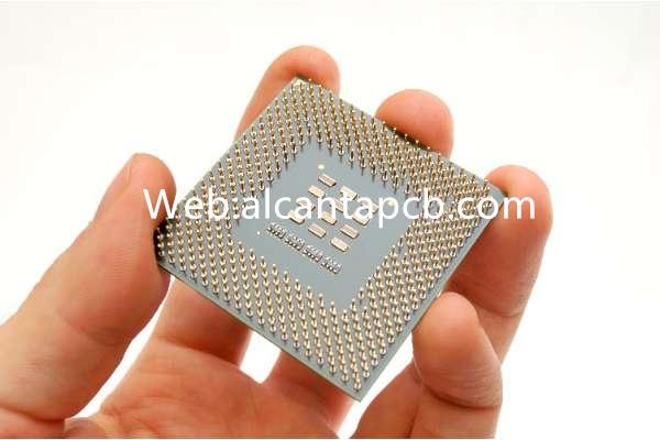
Ultradünnes Ball Grid Array (BGA) Substrate sind wesentliche Komponenten bei der Verpackung integrierter Schaltkreise (ICs), insbesondere bei Anwendungen mit hoher Dichte und hoher Leistung. Diese Substrate bieten eine hervorragende elektrische und thermische Leistung und minimieren gleichzeitig die Gesamtgröße und das Gewicht des Elektronikpakets. Ultradünne BGA-Substrate werden zunehmend in der modernen Elektronik eingesetzt, wie Smartphones, Laptops, und andere tragbare Geräte, wo Platz und Leistung entscheidende Faktoren sind.
Was ist ein ultradünnes BGA-Substrat??
Ein ultradünnes BGA-Substrat ist eine Art Substrat, das bei der Verpackung von Halbleiterbauelementen verwendet wird. Es dient als Basis, auf der der Halbleiterchip montiert wird, und stellt die notwendigen elektrischen Verbindungen zwischen dem Chip und der Leiterplatte her (Leiterplatte). Der “ultradünn” Der Aspekt bezieht sich auf die geringere Dicke des Substrats im Vergleich zu herkömmlichen BGA-Substraten, Dies ermöglicht kompaktere und leichtere Elektronikpakete.
Bei der BGA-Verpackung werden Lotkugeln in einem Gittermuster auf der Unterseite des Substrats platziert, mit denen beim Reflow-Lötprozess elektrische Verbindungen zur Leiterplatte hergestellt werden. Ultradünne BGA-Substrate behalten die gleiche Funktionalität bei, bieten jedoch eine geringere Dicke, Damit eignen sie sich ideal für Anwendungen, bei denen der Platz knapp ist.
Referenzhandbuch zum Design ultradünner BGA-Substrate
Beim Entwurf eines ultradünnen BGA-Substrats sind mehrere wichtige Überlegungen erforderlich, um optimale Leistung und Zuverlässigkeit sicherzustellen. In den folgenden Abschnitten werden die wesentlichen Aspekte des ultradünnen BGA-Substratdesigns erläutert.
Während der Entwurfsphase müssen mehrere wichtige Überlegungen berücksichtigt werden:
Impedanzkontrolle: Eine präzise Impedanzkontrolle ist für die Aufrechterhaltung der Signalintegrität bei hohen Frequenzen unerlässlich. Dies erfordert eine sorgfältige Gestaltung der Signalspuren und die Verwendung von Materialien mit kontrollierter Impedanz.
Thermalmanagement: Ein effektives Wärmemanagement ist für Hochleistungsanwendungen von entscheidender Bedeutung. Das Design muss thermische Durchkontaktierungen beinhalten, Kühlkörper, oder andere Techniken zur effizienten Wärmeableitung.
Mechanische Stabilität: Das Substrat muss eine robuste mechanische Unterstützung bieten, um thermischen Zyklen und mechanischen Belastungen während des Betriebs standzuhalten.
Zuverlässigkeit: Durch den Einsatz hochwertiger Materialien und präziser Herstellungsverfahren wird eine langfristige Zuverlässigkeit gewährleistet, Vermeidung von Problemen wie Delaminierung und Verformung.
Welche Materialien werden in ultradünnen BGA-Substraten verwendet??
Die in ultradünnen BGA-Substraten verwendeten Materialien werden aufgrund ihrer komplementären Eigenschaften ausgewählt, um die Gesamtleistung des Substrats zu verbessern:
Hochleistungslaminate: Bietet mechanische Festigkeit und thermische Stabilität und behält gleichzeitig ein dünnes Profil bei. Zu den gängigen Materialien gehört Polyimid, Flüssigkristallpolymer (LCP), und Hochtemperatur-FR-4.
Ultradünne Kupferfolien: Wird für die leitfähigen Schichten verwendet, Bietet hervorragende elektrische Leitfähigkeit und Zuverlässigkeit.
Verlustarme Dielektrika: Wird verwendet, um die Leiterbahnen zu isolieren und die Signalintegrität aufrechtzuerhalten.
Fortschrittliche Klebstoffe: Verkleben Sie die Schichten miteinander und sorgen Sie für mechanische Stabilität.
Welche Größe haben ultradünne BGA-Substrate??
Die Größe ultradünner BGA-Substrate variiert je nach Anwendung und spezifischen Designanforderungen:
Dicke: Ultradünne BGA-Substrate haben typischerweise eine Dicke im Bereich von 50 Zu 200 Mikrometer, je nach Design und Anwendungsanforderungen.
Abmessungen: Die Länge und Breite der Substrate werden durch die Größe des Halbleiterchips und das Layout des Systems bestimmt. Sie können von kleinen Formfaktoren für kompakte Geräte bis hin zu größeren Substraten für komplexere elektronische Systeme reichen.
Der Herstellungsprozess ultradünner BGA-Substrate
Der Herstellungsprozess ultradünner BGA-Substrate umfasst mehrere präzise und kontrollierte Schritte, um eine hohe Qualität und Leistung sicherzustellen:
Hochwertige Laminate, Kupferfolien, und Klebstoffe werden ausgewählt und für die Verarbeitung vorbereitet. Die Materialien werden gereinigt und behandelt, um eventuelle Verunreinigungen zu entfernen und eine glatte Oberfläche zu gewährleisten.
Die Schichten des Substrats werden durch Hitze und Druck miteinander laminiert. Dieser Schritt stellt sicher, dass die Schichten sicher miteinander verbunden sind und das Substrat sein dünnes Profil behält.
Die leitenden Schichten werden strukturiert und geätzt, um die notwendigen elektrischen Leiterbahnen zu schaffen. Dabei werden Photolithographie- und chemische Ätztechniken eingesetzt, um präzise und genaue Muster zu erzielen.
Löcher werden in das Substrat gebohrt, um Durchkontaktierungen für elektrische Verbindungen zwischen den Schichten zu schaffen. Anschließend werden die Vias mit Kupfer plattiert, um eine zuverlässige elektrische Leitfähigkeit zu gewährleisten.
Lotkugeln werden in einem Gittermuster auf der Unterseite des Substrats platziert. Diese Kugeln werden verwendet, um während des Reflow-Lötprozesses elektrische Verbindungen zur Leiterplatte herzustellen.
Nach der Herstellung, Das Substrat wird mit dem Halbleiterchip und allen erforderlichen Komponenten und Anschlüssen zusammengebaut. Es werden strenge Tests durchgeführt, um sicherzustellen, dass das Substrat alle Designspezifikationen und Leistungsanforderungen erfüllt. Dazu gehört auch die Prüfung der elektrischen Leistung, Wärmemanagement, und mechanische Integrität.
Der Anwendungsbereich ultradünner BGA-Substrate
Ultradünne BGA-Substrate werden in einer Vielzahl von Hochleistungsanwendungen eingesetzt:
In mobilen Geräten wie Smartphones und Tablets, Ultradünne BGA-Substrate bieten die erforderliche Leistung und kompakte Größe, um erweiterte Funktionen zu unterstützen und gleichzeitig die Gesamtdicke des Geräts zu minimieren.
In tragbarer Elektronik, Ultradünne BGA-Substrate ermöglichen die Integration fortschrittlicher Funktionen in kompakte und leichte Formfaktoren, Gewährleistung von Komfort und Benutzerfreundlichkeit für den Träger.
In Hochleistungsrechneranwendungen, Ultradünne BGA-Substrate bieten die notwendige elektrische und thermische Leistung, um die erweiterten Verarbeitungsfähigkeiten moderner CPUs und GPUs zu unterstützen.
In Telekommunikationsgeräten, Ultradünne BGA-Substrate werden verwendet, um die Hochfrequenz- und Hochleistungsanforderungen fortschrittlicher Kommunikationssysteme zu unterstützen.
In der Automobilelektronik, Ultradünne BGA-Substrate bieten die Zuverlässigkeit und Leistung, die für fortschrittliche Fahrerassistenzsysteme erforderlich sind (Adas) und andere elektronische Systeme in Fahrzeugen.
Was sind die Vorteile ultradünner BGA-Substrate??
Ultradünne BGA-Substrate bieten mehrere Vorteile, die sie für Hochleistungsanwendungen unverzichtbar machen:
Kompakte Größe: Ultradünne BGA-Substrate ermöglichen das Design kompakter und leichter Elektronikgehäuse, Ideal für tragbare und platzbeschränkte Anwendungen.
Hohe elektrische Leistung: Ultradünne BGA-Substrate bieten eine hervorragende elektrische Leistung bei minimalem Signalverlust und hoher Signalintegrität.
Effizientes Wärmemanagement: Ultradünne BGA-Substrate sorgen für ein effizientes Wärmemanagement, Wärme effektiv ableiten und die Leistung von Hochleistungskomponenten aufrechterhalten.
Mechanische Stabilität: Ultradünne BGA-Substrate bieten robusten mechanischen Halt, Temperaturschwankungen und mechanischen Belastungen während des Betriebs standhalten.
Vielseitigkeit: Ultradünne BGA-Substrate können in einer Vielzahl von Anwendungen eingesetzt werden, von mobilen Geräten bis hin zu Hochleistungsrechnern und Automobilelektronik.
FAQ
Was sind die wichtigsten Überlegungen beim Entwurf eines ultradünnen BGA-Substrats??
Zu den wichtigsten Überlegungen gehört die Materialauswahl hinsichtlich der thermischen und elektrischen Leistung, Schichtaufbau für Signalintegrität und Wärmemanagement, und Gewährleistung mechanischer Stabilität und Zuverlässigkeit.
Wie unterscheiden sich ultradünne BGA-Substrate von herkömmlichen BGA-Substraten??
Ultradünne BGA-Substrate haben im Vergleich zu herkömmlichen BGA-Substraten eine geringere Dicke, Dies ermöglicht kompaktere und leichtere Elektronikpakete bei gleichbleibender Funktionalität.
Was ist der typische Herstellungsprozess für ultradünne BGA-Substrate??
Der Prozess beinhaltet die Materialvorbereitung, Schichtlaminierung, Musterung und Radierung, Bohren und Beschichten, Lötkugelaufsatz, und strenge Montage und Tests, um hohe Qualität und Leistung sicherzustellen.
Was sind die Hauptanwendungen ultradünner BGA-Substrate??
Ultradünne BGA-Substrate werden in mobilen Geräten verwendet, tragbare Elektronik, Hochleistungs-Computing, Telekommunikationsgeräte, und Automobilelektronik, Bietet erweiterte Funktionalität und Zuverlässigkeit in kompakten Formfaktoren.