КОМПАНИЯ С ОГРАНИЧЕННОЙ ОТВЕТСТВЕННОСТЬЮ")
Ультратонкий BGA субстраты Производитель.Мы являемся ведущим производителем ультратонких подложек BGA., специализирующийся на производстве высокопроизводительных, миниатюрные решения для передовых электронных приложений. Наши современные производственные процессы обеспечивают превосходное качество и надежность., удовлетворение требований современных технологий в таких отраслях, как телекоммуникации, вычисления, и бытовая электроника.
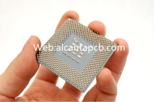
Ультратонкий массив шариковых сеток (БГА) субстраты являются важными компонентами упаковки интегральных схем. (ИС), особенно в приложениях с высокой плотностью и производительностью. Эти подложки обеспечивают превосходные электрические и тепловые характеристики при минимизации общего размера и веса электронного корпуса.. Ультратонкие подложки BGA все чаще используются в современной электронике., например, смартфоны, ноутбуки, и другие портативные устройства, где пространство и производительность имеют решающее значение.
Что такое ультратонкая подложка BGA??
Ультратонкая подложка BGA — это тип подложки, используемой при упаковке полупроводниковых устройств.. Он служит основой, на которой монтируется полупроводниковый кристалл, и обеспечивает необходимые электрические соединения между кристаллом и печатной платой. (печатная плата). The “ультратонкий” аспект относится к уменьшенной толщине подложки по сравнению с традиционными подложками BGA., создание более компактных и легких электронных блоков.
Упаковка BGA предполагает размещение шариков припоя в виде сетки на нижней поверхности подложки., которые используются для создания электрических соединений с печатной платой во время процесса пайки оплавлением.. Ультратонкие подложки BGA сохраняют ту же функциональность, но имеют меньшую толщину., что делает их идеальными для приложений, где пространство имеет большое значение.
Справочное руководство по проектированию сверхтонких подложек BGA
При разработке сверхтонкой подложки BGA необходимо учитывать несколько ключевых факторов, обеспечивающих оптимальную производительность и надежность.. В следующих разделах описаны основные аспекты проектирования сверхтонких подложек BGA..
На этапе проектирования необходимо учитывать несколько ключевых соображений.:
Контроль импеданса: Точный контроль импеданса необходим для поддержания целостности сигнала на высоких частотах.. Это предполагает тщательную разработку трасс сигнала и использование материалов с контролируемым импедансом..
Управление температурным режимом: Эффективное управление температурным режимом имеет решающее значение для приложений с высокой мощностью.. В конструкции должны быть предусмотрены тепловые переходы., радиаторы, или другие методы для эффективного рассеивания тепла.
Механическая стабильность: Подложка должна обеспечивать надежную механическую поддержку, чтобы выдерживать термоциклирование и механические нагрузки во время эксплуатации..
Надежность: Долгосрочная надежность обеспечивается за счет использования высококачественных материалов и точных производственных процессов., предотвращение таких проблем, как расслоение и деформация.
Какие материалы используются в ультратонких подложках BGA?
Материалы, используемые в ультратонких подложках BGA, выбираются на основе их взаимодополняющих свойств, позволяющих улучшить общие характеристики подложки.:
Высокопроизводительные ламинаты: Обеспечивает механическую прочность и термическую стабильность, сохраняя при этом тонкий профиль.. Общие материалы включают полиимид., жидкокристаллический полимер (LCP), и высокотемпературный ФР-4.
Ультратонкая медная фольга: Используется для проводящих слоев, обеспечение превосходной электропроводности и надежности.
Диэлектрики с низкими потерями: Используется для изоляции проводящих дорожек и поддержания целостности сигнала..
Усовершенствованные клеи: Скрепите слои вместе и обеспечьте механическую стабильность..
Какой размер имеют ультратонкие подложки BGA??
Размер ультратонких подложек BGA варьируется в зависимости от применения и конкретных требований к проектированию.:
Толщина: Ультратонкие подложки BGA обычно имеют толщину от 50 к 200 микрометры, в зависимости от конструкции и требований применения.
Размеры: Длина и ширина подложек определяются размером полупроводникового кристалла и компоновкой системы.. Они могут варьироваться от малых форм-факторов для компактных устройств до более крупных подложек для более сложных электронных систем..
Процесс производства ультратонких подложек BGA
Процесс производства ультратонких подложек BGA включает в себя несколько точных и контролируемых этапов, обеспечивающих высокое качество и производительность.:
Качественный ламинат, медная фольга, и клеи выбраны и подготовлены к обработке. Материалы очищаются и обрабатываются для удаления любых примесей и обеспечения гладкой поверхности..
Слои подложки ламинируются вместе с помощью тепла и давления.. Этот шаг обеспечивает надежное соединение слоев и сохранение тонкого профиля подложки..
Проводящие слои имеют рисунок и протравлены для создания необходимых электрических путей.. Это предполагает использование методов фотолитографии и химического травления для достижения точных и точных рисунков..
В подложке сверлятся отверстия для создания переходных отверстий для электрических соединений между слоями.. Затем переходные отверстия покрываются медью для обеспечения надежной электропроводности..
Шарики припоя размещаются в виде сетки на нижней поверхности подложки.. Эти шарики будут использоваться для создания электрических соединений с печатной платой во время процесса пайки оплавлением..
После изготовления, подложка собирается с полупроводниковым кристаллом и всеми необходимыми компонентами и разъемами.. Проводятся строгие испытания, чтобы гарантировать, что подложка соответствует всем проектным спецификациям и требованиям к производительности.. Сюда входит проверка электрических характеристик., управление температурным режимом, и механическая целостность.
Область применения ультратонких подложек BGA
Ультратонкие подложки BGA используются в широком спектре высокопроизводительных приложений.:
На мобильных устройствах, таких как смартфоны и планшеты., ультратонкие подложки BGA обеспечивают необходимую производительность и компактный размер для поддержки расширенных функций при минимальной общей толщине устройства..
В носимой электронике, ультратонкие подложки BGA позволяют интегрировать расширенные функции в компактные и легкие форм-факторы, обеспечение комфорта и удобства использования для пользователя.
В высокопроизводительных вычислительных приложениях, ультратонкие подложки BGA обеспечивают необходимые электрические и тепловые характеристики для поддержки расширенных вычислительных возможностей современных процессоров и графических процессоров..
В телекоммуникационном оборудовании, ультратонкие подложки BGA используются для обеспечения высокочастотных и мощных требований современных систем связи..
В автомобильной электронике, Ультратонкие подложки BGA обеспечивают надежность и производительность, необходимые для современных систем помощи водителю. (АДАС) и другие электронные системы транспортных средств.
Каковы преимущества ультратонких подложек BGA??
Ультратонкие подложки BGA обладают рядом преимуществ, которые делают их незаменимыми в высокопроизводительных приложениях.:
Компактный размер: Ультратонкие подложки BGA позволяют создавать компактные и легкие электронные корпуса., идеально подходит для портативных приложений и приложений с ограниченным пространством.
Высокие электрические характеристики: Ультратонкие подложки BGA обеспечивают превосходные электрические характеристики с минимальными потерями сигнала и высокой целостностью сигнала..
Эффективное управление температурным режимом: Ультратонкие подложки BGA обеспечивают эффективное управление температурным режимом., эффективное рассеивание тепла и поддержание производительности мощных компонентов.
Механическая стабильность: Ультратонкие подложки BGA обеспечивают надежную механическую поддержку., выдерживает термоциклирование и механические нагрузки во время эксплуатации.
Универсальность: Ультратонкие подложки BGA можно использовать в широком спектре приложений., от мобильных устройств до высокопроизводительных компьютеров и автомобильной электроники.
Часто задаваемые вопросы
Каковы ключевые факторы при разработке ультратонкой подложки BGA??
Ключевые соображения включают выбор материала с учетом тепловых и электрических характеристик., стек слоев для обеспечения целостности сигнала и управления температурным режимом, и обеспечение механической стабильности и надежности.
Чем ультратонкие подложки BGA отличаются от традиционных подложек BGA?
Ультратонкие подложки BGA имеют меньшую толщину по сравнению с традиционными подложками BGA., создание более компактных и легких электронных блоков при сохранении той же функциональности.
Каков типичный процесс производства ультратонких подложек BGA??
Процесс предполагает подготовку материала., послойное ламинирование, Паттерн и травление, сверление и обшивка, крепление шарика припоя, строгая сборка и тестирование для обеспечения высокого качества и производительности..
Каковы основные области применения ультратонких подложек BGA??
Ультратонкие подложки BGA используются в мобильных устройствах, носимая электроника, Высокопроизводительные вычисления, телекоммуникационное оборудование, и автомобильная электроника, обеспечение расширенной функциональности и надежности в компактном форм-факторе.