КОМПАНИЯ С ОГРАНИЧЕННОЙ ОТВЕТСТВЕННОСТЬЮ")
Ultrathin IC Подложки упаковки Manufacturer.We are a leading manufacturer of ultrathin IC package substrates, предоставление передовых решений для высокопроизводительных электронных устройств. Наши передовые технологии производства обеспечивают исключительное качество., обеспечение миниатюризации и расширенной функциональности в различных приложениях, от смартфонов до медицинских устройств. Доверьте нам инновационные, надежный, and efficient IC package substrates that meet the demands of today’s technology-driven world.
Ultrathin IC (Интегральная схема) упаковка субстраты are a vital component in modern electronics, enabling the miniaturization and enhanced performance of various devices. These substrates are engineered to be extremely thin while maintaining the necessary electrical, термический, and mechanical properties to support high-performance ICs. Ultrathin substrates are particularly important in applications where space is at a premium, например, смартфоны, носимые устройства, и передовые вычислительные системы.
What is an Ultrathin IC Package Substrate?
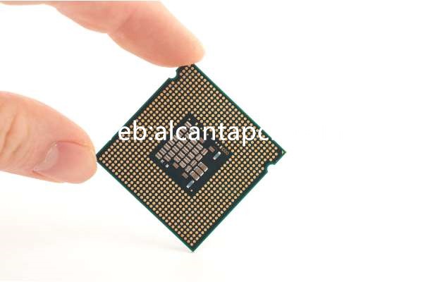
An ultrathin IC package substrate is a specialized type of printed circuit board (печатная плата) designed to provide a platform for mounting and interconnecting ICs. Эти подложки характеризуются минимальной толщиной., typically less than 100 микрометры, which allows for the development of ultra-compact electronic packages. Несмотря на свою худобу, ultrathin substrates must support high-density interconnections, Эффективное тепловое управление, and robust mechanical stability to ensure the reliable operation of the ICs they host.
Ultrathin IC Package Substrate Design Reference Guide
Designing ultrathin IC package substrates involves a comprehensive approach to ensure optimal performance and reliability.
The selection of materials is critical for achieving the desired properties in ultrathin substrates:
High-Density Polyimide Films: These materials offer excellent flexibility, высокая термическая стабильность, and good electrical insulation, making them ideal for ultrathin applications.
Медная фольга: Used for conductive traces and interconnections, copper foils must be thin yet durable to maintain electrical performance without adding significant bulk.
Adhesives and Dielectrics: Advanced adhesives and dielectric materials with low dielectric constants and high thermal conductivity are used to bond the layers and provide insulation.
The layer structure of ultrathin substrates is designed to maximize space efficiency and performance:
Сигнальные слои: These layers are configured to minimize signal loss and crosstalk. Techniques such as microstrip and stripline are used to maintain controlled impedance.
Слои питания и земли: Dedicated power and ground planes are crucial for stable power distribution and noise reduction, ensuring reliable IC operation.
Слои терморегулирования: Integrating thermal vias and heat spreaders helps to dissipate heat effectively, предотвращение перегрева критически важных компонентов.
Interconnect Layers: High-density interconnects (ИЧР) with microvias and through-holes enable complex routing within the constrained space of ultrathin substrates.
What Materials are Used in Ultrathin IC Package Substrates?
Materials used in ultrathin IC package substrates are selected for their ability to meet stringent performance requirements:
High-Density Polyimide Films: Offering excellent flexibility, термическая стабильность, и электроизоляция, these films are a common choice for ultrathin applications.
Медная фольга: Thin yet durable copper foils are used for conductive traces and interconnections, ensuring reliable electrical performance.
Adhesives and Dielectrics: Advanced adhesives and dielectric materials with low dielectric constants and high thermal conductivity are used to bond the layers and provide insulation.
Reinforced Epoxy Resins: These materials enhance the mechanical strength of the substrate while maintaining a low profile.
What Size are Ultrathin IC Package Substrates?
The size of ultrathin IC package substrates varies depending on the specific application and device requirements:
Толщина: Ultrathin substrates are typically less than 100 микрометры толщиной, with some designs reaching even lower thicknesses to accommodate the smallest form factors.
Длина и ширина: These dimensions are determined by the size of the IC and the layout of the interconnections. Typical sizes range from a few millimeters for small ICs to several centimeters for larger packages.
The Manufacturing Process of Ultrathin IC Package Substrates
The manufacturing process for ultrathin IC package substrates involves several precise and controlled steps to ensure high quality and performance:
High-density polyimide films, проводящие материалы, и клеи подготавливаются и разрезаются на соответствующие размеры для обработки..
Слои изготавливаются путем ламинирования проводящих и изоляционных материалов в стопку.. На каждом слое нанесен рисунок с использованием фотолитографии для определения схемы..
Микроотверстия и сквозные отверстия сверлятся с использованием лазерных или механических методов сверления.. Эти отверстия затем покрываются медью для создания электрических соединений между слоями..
Процессы фотолитографии и травления используются для создания микросхем на каждом слое.. This step requires high precision to ensure accurate and reliable interconnections.
After layer fabrication, the layers are laminated together under heat and pressure. The assembled substrate undergoes rigorous testing, включая электрические испытания, термоциклирование, и механические стресс-тесты, to ensure performance and reliability.
The Application Area of Ultrathin IC Package Substrates
Ultrathin IC package substrates enable advanced capabilities in a wide range of applications:
В смартфонах, таблетки, и носимые устройства, ultrathin substrates support the compact and efficient integration of advanced ICs, enhancing performance and functionality while reducing size and weight.
На серверах, центры обработки данных, and supercomputers, ultrathin substrates enable the integration of powerful processors and memory modules in a compact form factor, facilitating fast data processing and storage.
These substrates are essential in telecommunications infrastructure, including base stations and network equipment, providing reliable and high-speed connectivity in a compact footprint.
In various consumer electronics, from smart home devices to gaming consoles, ultrathin substrates enable high performance in sleek, space-efficient designs.
In medical imaging and diagnostic equipment, ultrathin substrates support high-speed data acquisition and processing, improving accuracy and efficiency in medical procedures.
What are the Advantages of Ultrathin IC Package Substrates?
Ultrathin IC package substrates offer several advantages that make them indispensable for advanced electronic applications:
Компактный дизайн: The ultra-thin profile allows for the miniaturization of electronic packages, enabling more compact and portable devices.
Высокая производительность: Optimized materials and design ensure high signal integrity, low power loss, и эффективное управление температурным режимом.
Повышенная надежность: Advanced manufacturing processes and materials provide high reliability, ensuring long-term performance in demanding environments.
Гибкость: The thin and flexible nature of these substrates makes them suitable for a wide range of applications, from rigid high-performance devices to flexible and wearable electronics.
Масштабируемость: Ultrathin substrates can be customized to meet the specific needs of various applications, from small consumer devices to large industrial systems.
Часто задаваемые вопросы
What are the key considerations in designing ultrathin IC package substrates?
Key considerations include material selection for electrical and thermal properties, layer structure optimization for signal integrity and thermal management, и обеспечение механической стабильности и надежности.
How do ultrathin IC package substrates differ from standard PCBs?
Ultrathin IC package substrates are significantly thinner, with more layers and higher interconnect density, designed to handle higher frequencies and power levels compared to standard PCBs, making them suitable for advanced applications.
What is the typical manufacturing process for ultrathin IC package substrates?
Процесс предполагает подготовку материала., изготовление слоев, сверление и обшивка, создание схем, сборка, и строгие испытания для обеспечения высокой производительности и надежности.
What are the main applications of ultrathin IC package substrates?
These substrates are used in mobile devices, Высокопроизводительные вычисления, телекоммуникации, потребительская электроника, и медицинское оборудование, providing advanced functionality and reliability in these fields.