CO.,LTD")
Hersteller von Wire-Bonding-IC-Substraten. Als führender Hersteller von Wire-Bonding-IC-Substraten, Wir sind auf die Herstellung von Hochleistungssubstraten spezialisiert, die zuverlässige Verbindungen und optimale elektrische Leistung gewährleisten. Unsere fortschrittlichen Herstellungsprozesse und strengen Qualitätskontrollstandards garantieren Substrate, die den höchsten Branchenanforderungen entsprechen, Unterstützung einer breiten Palette von Anwendungen in der Elektronik.
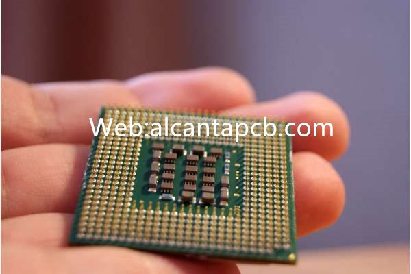
Wire-Bonding-IC-Substrate sind wesentliche Komponenten in der Halbleiterverpackung, Bereitstellung der notwendigen elektrischen Verbindungen zwischen dem Siliziumchip und den externen Schaltkreisen. Diese Substrate dienen als Plattform für den Drahtbondprozess, Dabei verbinden feine Metalldrähte den Chip mit dem Substrat, Ermöglicht den Fluss elektrischer Signale. Das Design und die Materialzusammensetzung dieser Substrate sind entscheidend für die Gewährleistung der Zuverlässigkeit, Leistung, und Langlebigkeit des integrierten Schaltkreises (IC) Paket, insbesondere bei Hochleistungsanwendungen.
Was sind Wire-Bonding-IC-Substrate??
Drahtbond-IC-Substrate sind spezielle Leiterplatten oder Träger, die den Siliziumchip halten und durch Drahtbondtechniken mit externen Schaltkreisen verbinden. Drahtbonden ist eine der gebräuchlichsten Methoden zur Herstellung elektrischer Verbindungen in Halbleiterbauelementen. Dabei wird Feingold angebracht, Aluminium, oder Kupferdrähte von den Bondpads auf dem Siliziumchip zu den entsprechenden Pads auf dem Substrat. Diese Drähte bilden die entscheidenden elektrischen Pfade, die es dem Chip ermöglichen, mit anderen Komponenten in einem System zu kommunizieren.
Das Substrat selbst ist eine mehrschichtige Struktur aus verschiedenen Materialien, einschließlich organischer Laminate, Keramik, oder Metalle, je nach Anwendung und geforderten Leistungsmerkmalen. Die Wahl von Substrat Material ist wichtig, da es die Thermik beeinflusst, mechanisch, und elektrische Eigenschaften des IC-Gehäuses. Wichtige Eigenschaften wie der Wärmeausdehnungskoeffizient (CTE), Dielektrizitätskonstante, und Wärmeleitfähigkeit werden bei der Substratauswahl sorgfältig berücksichtigt, um die Kompatibilität mit dem Chip und dem gesamten Gehäusedesign sicherzustellen.
Materialien, die beim Drahtbonden von IC-Substraten verwendet werden
Die für Drahtbond-IC-Substrate verwendeten Materialien werden auf der Grundlage ihrer Fähigkeit ausgewählt, den Drahtbondprozess zu unterstützen und gleichzeitig die gewünschte elektrische und thermische Leistung aufrechtzuerhalten. Zu den gängigen Materialien gehören::
Diese Substrate bestehen typischerweise aus Materialien wie FR4 oder BT (Bismaleimide Triazine) Harz, die in der Unterhaltungselektronik und in weniger anspruchsvollen Anwendungen weit verbreitet sind. Organische Laminate bieten gute elektrische Isolationseigenschaften und sind kostengünstig, Dadurch sind sie für die Massenproduktion geeignet. Jedoch, Ihre thermische Leistung kann im Vergleich zu anderen Materialien begrenzt sein.
Keramik Substrate, wie Aluminiumoxid (AL2O3) oder Aluminiumnitrid (AlN), werden überall dort eingesetzt, wo eine hohe Wärmeleitfähigkeit und mechanische Stabilität erforderlich sind. Keramik bietet hervorragende Wärmemanagementfähigkeiten und wird häufig in Hochleistungs- oder Hochzuverlässigkeitsanwendungen eingesetzt, beispielsweise in der Automobil- oder Luft- und Raumfahrtelektronik. Diese Materialien sind auch mit Fine-Pitch-Drahtbonden kompatibel, Damit eignen sie sich ideal für fortschrittliche IC-Pakete.
In einigen Hochleistungsanwendungen, Metallkernsubstrate werden verwendet, um zusätzliche mechanische Festigkeit und verbesserte Wärmeableitung zu gewährleisten. Diese Substrate bestehen typischerweise aus einem Metallkern, wie Kupfer oder Aluminium, mit Isolierschichten laminiert. Metallkernsubstrate sind besonders in der Leistungselektronik nützlich, wo eine effiziente Wärmeableitung entscheidend ist, um thermische Ausfälle zu verhindern.
Für Anwendungen, die ein ausgewogenes Verhältnis von Leistung und Kosten erfordern, Es können fortschrittliche Verbundwerkstoffe verwendet werden. Diese Verbundwerkstoffe vereinen die Vorteile organischer und keramischer Materialien, bieten eine gute thermische und elektrische Leistung und sind gleichzeitig kostengünstiger als reine Keramiksubstrate. Fortschrittliche Verbundwerkstoffe werden häufig in Telekommunikations- und Hochfrequenzanwendungen eingesetzt, bei denen die Signalintegrität von entscheidender Bedeutung ist.
Designüberlegungen für Drahtbond-IC-Substrate
Bei der Entwicklung von Drahtbond-IC-Substraten sind mehrere wichtige Überlegungen erforderlich, um sicherzustellen, dass das Endprodukt die erforderlichen Leistungs- und Zuverlässigkeitsstandards erfüllt:
Die Anordnung der Bondpads auf dem Substrat ist entscheidend für die Gewährleistung zuverlässiger Drahtbondverbindungen. Die Pads müssen mit präzisem Abstand und Ausrichtung positioniert werden, um den Drahtbondprozess zu ermöglichen und Probleme wie Drahtdurchhängen oder Kurzschlüsse zu vermeiden. Auch die Oberflächenbeschaffenheit des Pads ist wichtig, da es die Qualität der Drahtverbindung beeinflusst.
Beim Drahtbonden von IC-Substraten ist ein effektives Wärmemanagement unerlässlich, um eine Überhitzung des Chips und der Bonddrähte zu verhindern. Dies kann durch die Verwendung von Materialien mit hoher Wärmeleitfähigkeit erreicht werden, thermische Durchkontaktierungen, oder Kühlkörper. Durch das richtige thermische Design wird sichergestellt, dass die vom IC erzeugte Wärme effizient abgeleitet wird, Aufrechterhaltung der Leistung und Langlebigkeit des Pakets.
Die dielektrischen Eigenschaften des Substratmaterials beeinflussen die Signalintegrität und die Leistungsverteilung innerhalb des IC-Gehäuses. Für Hochfrequenzanwendungen werden Materialien mit niedriger Dielektrizitätskonstante und niedrigem Verlustfaktor bevorzugt, da sie Signalverluste und Übersprechen zwischen benachbarten Leiterbahnen minimieren. Um sicherzustellen, dass die dielektrischen Eigenschaften des Substrats den Anwendungsanforderungen entsprechen, ist es für die Aufrechterhaltung der Gesamtleistung des Gehäuses von entscheidender Bedeutung.
Die mechanische Stabilität des Substrats ist wichtig, um den Belastungen standzuhalten, die mit dem Drahtbonden und der anschließenden Handhabung des Gehäuses einhergehen. Das Substrat muss über ausreichende mechanische Festigkeit verfügen, um den Chip und die Bonddrähte zu tragen, ohne sich zu verziehen oder zu reißen. Zusätzlich, der Wärmeausdehnungskoeffizient (CTE) Die Stärke des Substrats sollte eng an die des Chips angepasst sein, um thermisch bedingte Spannungen zu vermeiden, die zu Verbindungsfehlern führen könnten.
Die Oberflächenbeschaffenheit der Bondpads auf dem Substrat ist ein Schlüsselfaktor im Drahtbondprozess. Zu den gängigen Oberflächen gehört Gold, Silber, oder Kupfer, wobei Gold aufgrund seiner hervorragenden Bindungseigenschaften und Oxidationsbeständigkeit am häufigsten verwendet wird. Die Wahl der Oberflächenbeschaffenheit beeinflusst die Haftfestigkeit und die Zuverlässigkeit der elektrischen Verbindungen.
Herstellungsprozess von IC-Substraten zum Drahtbonden
Der Herstellungsprozess von Wire-Bonding-IC-Substraten umfasst mehrere wichtige Schritte, Jedes dieser Elemente muss sorgfältig kontrolliert werden, um die Qualität und Leistung des Endprodukts sicherzustellen:
Der Prozess beginnt mit der Auswahl des geeigneten Substratmaterials basierend auf den Designanforderungen. Anschließend wird das Material gereinigt und in die gewünschte Form und Größe geschnitten.
Für mehrschichtige Untergründe, Schichten aus leitenden und isolierenden Materialien werden zusammenlaminiert, um den Substratstapel zu bilden. Bei diesem Prozess werden Hitze und Druck angewendet, um die Schichten miteinander zu verbinden, Schaffung eines festen und stabilen Untergrunds.
Das Schaltungsmuster wird durch Aufbringen eines Fotolacks auf dem Substrat erzeugt, indem man es durch eine Maske UV-Licht aussetzt, und dann das unerwünschte leitende Material wegätzen. Dieser Schritt definiert das Layout der Leiterbahnen und Bondpads auf dem Substrat.
Durch das Substrat werden Durchkontaktierungen gebohrt, um elektrische Verbindungen zwischen verschiedenen Schichten herzustellen. Anschließend werden die Durchkontaktierungen mit leitfähigem Material beschichtet, um zuverlässige elektrische Verbindungen zu gewährleisten. In einigen Fällen, Microvias können in Designs mit hoher Dichte verwendet werden, um ein komplexeres Routing zu ermöglichen.
Die Bondpads auf dem Untergrund sind mit einem Oberflächenfinish beschichtet, wie Gold oder Silber, um den Drahtbondprozess zu verbessern. Die Oberfläche muss gleichmäßig und fehlerfrei sein, um starke und zuverlässige Drahtverbindungen zu gewährleisten.
Die fertigen Substrate werden strengen Tests und Inspektionen unterzogen, um sicherzustellen, dass sie alle elektrischen Anforderungen erfüllen, mechanisch, und thermische Spezifikationen. Zu den Tests gehört die Überprüfung der Integrität der Drahtverbindungen, Prüfung auf Fehler im Substratmaterial, und Sicherstellen, dass das Substrat die erforderlichen Leistungsstandards erfüllt.
Anwendungen von Wire-Bonding-IC-Substraten
Drahtbond-IC-Substrate werden in einer Vielzahl von Halbleiterverpackungsanwendungen eingesetzt, einschließlich:
Drahtbondsubstrate werden häufig in der Unterhaltungselektronik eingesetzt, wie Smartphones, Tabletten, und tragbare Geräte. Diese Substrate stellen die notwendigen Verbindungen zwischen den ICs und den externen Komponenten bereit, die Funktionalität dieser Geräte zu ermöglichen.
In Automobilanwendungen, Drahtbondsubstrate werden in elektronischen Steuergeräten eingesetzt (ABDECKUNG), Sensoren, und Leistungsmodule. Diese Substrate müssen rauen Betriebsbedingungen standhalten, einschließlich hoher Temperaturen, Vibration, und Feuchtigkeit, Zuverlässigkeit ist ein zentraler Aspekt.
Drahtbondsubstrate sind wichtige Komponenten in Telekommunikationsgeräten, einschließlich Basisstationen, Router, und Transceiver. Diese Substrate unterstützen die für die drahtlose Kommunikation erforderlichen Hochfrequenzsignale, Gewährleistung der Signalintegrität und -zuverlässigkeit.
Drahtbondsubstrate werden in medizinischen Geräten verwendet, wie zum Beispiel Herzschrittmacher, bildgebende Systeme, und Diagnosegeräte. Diese Substrate müssen strenge Qualitäts- und Zuverlässigkeitsstandards erfüllen, um die Sicherheit und Wirksamkeit der medizinischen Geräte zu gewährleisten.
Vorteile von Wire-Bonding-IC-Substraten
Drahtbond-IC-Substrate bieten mehrere Vorteile, die sie zu einer bevorzugten Wahl für Halbleitergehäuse machen:
Drahtbondsubstrate sind mit einer Vielzahl von IC-Designs kompatibel und können in verschiedenen Anwendungen eingesetzt werden, von Unterhaltungselektronik bis hin zu Automobil und Telekommunikation.
Der Drahtbondprozess ist im Vergleich zu anderen Methoden im Allgemeinen kostengünstiger, wie zum Beispiel Flip-Chip-Bonding, Dadurch eignet es sich für die Massenproduktion.
Drahtbondsubstrate sind darauf ausgelegt, zuverlässige elektrische Verbindungen bereitzustellen, die den Strapazen des Betriebs standhalten, einschließlich Temperaturwechsel, Vibration, und Umweltexposition.
Drahtbond-Substrate können leicht skaliert werden, um unterschiedliche Die-Größen und Schaltungskomplexitäten zu berücksichtigen, Dadurch eignen sie sich für eine breite Palette von Halbleitergehäusen.
FAQ
Welches sind die am häufigsten verwendeten Materialien für IC-Substrate zum Drahtbonden??
Zu den gängigsten Materialien gehören organische Laminate (wie FR4 und BT-Harz), Keramik (wie Aluminiumoxid und Aluminiumnitrid), und Metallkernsubstrate.
Warum ist das Wärmemanagement beim Drahtbonden von IC-Substraten wichtig??
Das Wärmemanagement ist entscheidend, um eine Überhitzung des Chips und der Bonddrähte zu verhindern, Dies kann zu Ausfällen und verminderter Zuverlässigkeit führen. Das richtige thermische Design sorgt für eine effiziente Wärmeableitung und erhält die Leistung des Gehäuses aufrecht.
Für welche Anwendungen werden typischerweise Wire-Bonding-IC-Substrate verwendet??
Drahtbond-IC-Substrate werden in der Unterhaltungselektronik eingesetzt, Automobilelektronik, Telekommunikation, und medizinische Geräte, unter anderem Anwendungen.
Wie wirkt sich die Oberflächenbeschaffenheit des Substrats auf den Drahtbondprozess aus??
Die Oberflächenbeschaffenheit, typischerweise Gold oder Silber, wirkt sich auf die Verbindungsstärke und Zuverlässigkeit der Drahtverbindungen aus. Eine hochwertige Verarbeitung sorgt für starke und langlebige Verbindungen.