CO., LTD")
18 Fabricante de sustrato de capa BGA/IC. Un BGA/IC de 18 capas sustrato El fabricante se especializa en producir sustratos de alto rendimiento para circuitos integrados Ball Grid Array. (BGA/IC). Estos sustratos son esenciales para envases electrónicos avanzados, ofreciendo múltiples capas para admitir diseños de circuitos complejos. La empresa garantiza la precisión en la fabricación y el control de calidad., proporcionando soluciones robustas y confiables para aplicaciones de alta densidad en diversas industrias, incluyendo electrónica de consumo y telecomunicaciones. Su experiencia en tecnología multicapa cumple con estrictos estándares industriales., asegurando un rendimiento y durabilidad óptimos.
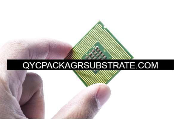
Cuáles son 18 Capa de sustratos BGA/IC?
Un 18 El sustrato Layer BGA/IC es un tipo altamente especializado de placa de circuito impreso. (tarjeta de circuito impreso) diseñado para soportar Ball Grid Array (BGA) paquetes y circuitos integrados (IM) con un alto nivel de complejidad y funcionalidad. El “18 capa” La designación se refiere al número de capas conductoras dentro del sustrato., que se utilizan para enrutar señales eléctricas, distribuyendo poder, y gestionar el rendimiento térmico. Estos sustratos son críticos en la electrónica avanzada., donde la alta densidad, miniaturización, y la confiabilidad son primordiales.
La función principal de un 18 El sustrato Layer BGA/IC proporciona una plataforma estable y eficiente para montar componentes BGA e IC.. Las múltiples capas dentro del sustrato permiten las interconexiones complejas que requieren los dispositivos semiconductores modernos., permitiendo la integración de varias funcionalidades en un solo, paquete compacto. Esto es particularmente importante en aplicaciones como la informática de alto rendimiento., telecomunicaciones, y electrónica de consumo, donde el espacio es limitado, pero las exigencias de rendimiento son altas.
El diseño de estos sustratos implica una cuidadosa consideración de factores como la integridad de la señal., entrega de energía, y gestión térmica. El 18 Las capas generalmente están dispuestas para optimizar el rendimiento de los circuitos integrados., con capas específicas dedicadas a los planos de potencia y tierra, enrutamiento de señal, y disipación de calor. Esta estructura en capas permite la separación de diferentes tipos de señales., Minimizar las interferencias y garantizar un funcionamiento fiable..
Además de sus funciones eléctricas y térmicas, 18 Los sustratos Layer BGA/IC también proporcionan soporte mecánico para los componentes montados en ellos.. Los materiales utilizados en estos sustratos se eligen por su capacidad para resistir las tensiones de los ciclos térmicos y las vibraciones mecánicas., asegurando confiabilidad a largo plazo en entornos exigentes.
18 Guía de referencia de diseño de sustrato Layer BGA/IC
Diseñando un 18 El sustrato Layer BGA/IC es un proceso complejo que requiere una comprensión profunda de los requisitos eléctricos y mecánicos de la aplicación final.. El diseño comienza con la definición de las especificaciones de los circuitos integrados y paquetes BGA que se montarán en el sustrato., incluyendo sus configuraciones de pines, requisitos de energía, y características térmicas. De eso, El diseñador debe crear un diseño que enrute eficientemente las señales y la energía a través del 18 capas mientras minimiza la diafonía, pérdida de señal, y interferencia electromagnética (EMI).
El proceso de diseño implica la colocación cuidadosa de las vías., rastros, y planos dentro del sustrato. Se perforan vías a través de las capas para crear conexiones eléctricas entre ellas., mientras que las huellas son las vías conductoras que transportan señales y energía.. En un sustrato de 18 capas, El diseñador debe equilibrar la necesidad de un enrutamiento denso con la necesidad de mantener un espacio adecuado entre las pistas para evitar interferencias.. Los planos de alimentación y tierra están ubicados estratégicamente para proporcionar niveles de voltaje estables y proteger las señales sensibles del ruido..
A menudo se utilizan herramientas de simulación avanzadas durante el proceso de diseño para modelar el comportamiento eléctrico del sustrato en diversas condiciones operativas.. Estas herramientas permiten a los diseñadores optimizar el diseño para la integridad de la señal., Asegurar que las señales de alta velocidad puedan viajar a través del sustrato sin degradación.. Las simulaciones térmicas también son cruciales, ya que ayudan a identificar posibles puntos críticos dentro del sustrato y a diseñar soluciones de refrigeración adecuadas.
Además de las consideraciones eléctricas y térmicas, El diseño mecánico del sustrato debe tener en cuenta las tensiones que experimentará durante la fabricación y el funcionamiento.. La elección de los materiales juega aquí un papel fundamental., ya que deben poder soportar las altas temperaturas y fuerzas mecánicas asociadas con la soldadura y los ciclos térmicos.. El sustrato también debe ser lo suficientemente robusto como para resistir deformaciones o grietas durante el uso., especialmente en aplicaciones donde estará expuesto a un estrés mecánico significativo.
¿En qué material se utiliza? 18 Capa de sustratos BGA/IC?
Los materiales utilizados en 18 Los sustratos Layer BGA/IC se eligen por su capacidad para cumplir con los estrictos requisitos eléctricos., térmico, y requisitos mecánicos de aplicaciones electrónicas avanzadas. El material principal utilizado en el sustrato es un dieléctrico de alto rendimiento., típicamente un tipo de resina como epoxi o poliimida. Estos materiales proporcionan un excelente aislamiento eléctrico entre las capas conductoras y al mismo tiempo ofrecen la estabilidad mecánica necesaria para soportar la compleja estructura del sustrato..
El cobre es el material elegido para las pistas y planos conductores dentro del sustrato.. El cobre es altamente conductor., lo que lo hace ideal para transportar las señales eléctricas y la potencia que requieren los circuitos integrados.. Las capas de cobre suelen ser muy delgadas y están cuidadosamente modeladas utilizando técnicas de fotolitografía para crear intrincadas redes de trazas que conectan los distintos componentes del sustrato.. En algunos casos, El cobre puede estar recubierto con otros metales., como el níquel y el oro, para mejorar su durabilidad y garantizar conexiones de soldadura confiables.
Además de los materiales dieléctricos y conductores., 18 Los sustratos Layer BGA/IC también pueden incluir otros materiales para mejorar su rendimiento.. Por ejemplo, Se pueden agregar rellenos cerámicos a las capas dieléctricas para mejorar su conductividad térmica y ayudar a disipar el calor de los circuitos integrados.. Esto es especialmente importante en aplicaciones de alto rendimiento donde los componentes generan una cantidad significativa de calor..
El acabado superficial del sustrato es otra consideración crítica del material.. Acabados superficiales como oro por inmersión en níquel químico (Aceptar) o conservantes orgánicos de soldabilidad (OSP) Se aplican a las trazas de cobre para protegerlas de la oxidación y garantizar una buena soldabilidad.. Estos acabados son esenciales para mantener la confiabilidad a largo plazo de las uniones de soldadura entre el sustrato y los componentes..
¿Qué tamaño son? 18 Capa de sustratos BGA/IC?
El tamaño de un 18 El sustrato Layer BGA/IC depende en gran medida de la aplicación específica para la que está diseñado. A diferencia de los PCB estándar, que a menudo vienen en tamaños predefinidos, Estos sustratos suelen estar diseñados a medida para adaptarse a los requisitos del paquete electrónico que admiten.. Las dimensiones generales del sustrato pueden variar ampliamente., que van desde unos pocos milímetros hasta varios centímetros en cada lado, dependiendo de la complejidad y densidad de los circuitos que deben adaptarse.
En aplicaciones como la informática de alto rendimiento o las telecomunicaciones, donde los paquetes de circuitos integrados y BGA pueden ser grandes y numerosos, Es posible que el tamaño del sustrato deba ser correspondientemente mayor para proporcionar suficiente espacio para todas las conexiones necesarias.. En contraste, en aplicaciones donde la miniaturización es una preocupación clave, como en dispositivos móviles o implantes médicos, el sustrato podría diseñarse para que sea lo más pequeño posible manteniendo al mismo tiempo la funcionalidad requerida.
El espesor del sustrato es otra dimensión importante que varía según el diseño y la aplicación.. Un sustrato de 18 capas suele ser más grueso que los sustratos más simples debido a la cantidad de capas que contiene.. Sin embargo, Los diseñadores deben equilibrar cuidadosamente la necesidad de múltiples capas con la necesidad de mantener el sustrato lo suficientemente delgado como para ajustarse a las limitaciones del producto final.. Los sustratos más gruesos pueden ofrecer un mejor soporte mecánico y gestión térmica., pero también pueden ser más difíciles de integrar en dispositivos compactos.
La disposición de las capas dentro del sustrato también influye en su tamaño total.. Los diseñadores pueden optar por un diseño más compacto utilizando anchos de trazo más finos y espacios más ajustados., lo que permite una huella de sustrato más pequeña. Sin embargo, este enfoque requiere técnicas de fabricación avanzadas y puede aumentar el costo del sustrato. En cambio, un diseño más extendido puede ser más fácil y menos costoso de fabricar, pero puede resultar en un sustrato más grande.
El proceso de fabricación de 18 Capa de sustratos BGA/IC
El proceso de fabricación para 18 La capa de sustratos BGA/IC es compleja y requiere un alto grado de precisión y control.. El proceso comienza con la preparación de los materiales base., incluidas las capas dieléctricas y láminas de cobre que formarán el núcleo del sustrato. Estos materiales se laminan juntos bajo calor y presión para crear una estructura multicapa estable.. El número de capas y la disposición específica de los materiales se planifican cuidadosamente para cumplir con los requisitos eléctricos y térmicos del producto final..
Una vez preparada la estructura base, El sustrato se somete a una serie de pasos de fotolitografía para definir los patrones de circuito en cada capa.. Se aplica un material fotosensible llamado fotorresistente a la superficie de cobre., y el patrón deseado se expone usando ultravioleta (ultravioleta) luz. Luego se revelan las áreas expuestas del fotoprotector., y el cobre subyacente se elimina para crear la intrincada red de rastros que transportarán señales eléctricas a través del sustrato..
La perforación es otro paso crítico en el proceso de fabricación., donde se crean vías y orificios pasantes para establecer conexiones eléctricas entre las diferentes capas. Estos agujeros normalmente se perforan utilizando tecnología láser para lograr la precisión requerida para estructuras tan pequeñas y complejas.. Una vez perforado, Las vías están recubiertas de cobre para garantizar la conductividad a través de las capas..
Después de los procesos de perforación y grabado., el sustrato se somete a una serie de tratamientos superficiales para prepararlo para el ensamblaje de circuitos integrados y BGA. Esto incluye la aplicación de acabados superficiales como ENIG u OSP., que protegen las trazas de cobre de la oxidación y mejoran la soldabilidad. El sustrato también puede someterse a tratamientos adicionales para mejorar su rendimiento térmico., como la adición de vías térmicas o la aplicación de disipadores de calor.
Los pasos finales del proceso de fabricación implican pruebas e inspección.. El sustrato se prueba minuciosamente para garantizar que todas las conexiones eléctricas estén intactas y que no haya defectos que puedan comprometer su rendimiento.. Esto incluye pruebas eléctricas para verificar la integridad de la señal y la entrega de energía y pruebas mecánicas para garantizar que el sustrato pueda soportar las tensiones que encontrará durante el montaje y el funcionamiento..
El área de aplicación de 18 Capa de sustratos BGA/IC
18 Los sustratos Layer BGA/IC se utilizan en una variedad de aplicaciones de alto rendimiento., lo que refleja su capacidad para soportar circuitos electrónicos complejos y densamente empaquetados. Una de las áreas de aplicación más destacadas es la industria de los semiconductores., particularmente en tecnologías de embalaje avanzadas como BGA, chip invertido, y circuitos integrados 3D. Estos sustratos son esenciales para crear compactos., Paquetes de alta densidad que integran múltiples circuitos integrados y otros componentes en un solo, módulo eficiente.
En electrónica de consumo, 18 Los sustratos Layer BGA/IC se encuentran en dispositivos que requieren un alto nivel de rendimiento y confiabilidad., como teléfonos inteligentes, tabletas, y otros aparatos portátiles. Estos dispositivos se basan en sustratos que pueden acomodar una gran cantidad de conexiones en un espacio pequeño., al mismo tiempo que proporciona la gestión térmica necesaria para manejar el calor generado por los procesadores de alta velocidad y otros componentes..
La industria del automóvil es otro ámbito clave donde se utilizan estos sustratos, particularmente en aplicaciones relacionadas con sistemas avanzados de asistencia al conductor (ADA), infoentretenimiento, y unidades de control del motor (CUBRIR). Los sustratos en estas aplicaciones deben cumplir estándares estrictos de durabilidad y confiabilidad., ya que a menudo están expuestos a duras condiciones de funcionamiento, incluyendo temperaturas extremas, humedad, y vibraciones.
Las telecomunicaciones son un campo que se beneficia enormemente del uso de 18 Capa de sustratos BGA/IC, especialmente en el desarrollo de infraestructura 5G y otros sistemas de comunicación de alta frecuencia. Los sustratos en estas aplicaciones deben proporcionar una excelente integridad de la señal y gestión térmica para manejar las demandas de transmisión y procesamiento de datos de alta velocidad..
Los dispositivos médicos también utilizan 18 Capa de sustratos BGA/IC, particularmente en aplicaciones que requieren miniaturización y precisión, como dispositivos implantables, equipo de diagnostico, y monitores de salud portátiles. Estos sustratos ofrecen la biocompatibilidad, fiabilidad, y funcionalidad necesaria para aplicaciones médicas críticas, Garantizar que los dispositivos funcionen de forma precisa y fiable durante largos períodos..
¿Cuáles son las ventajas de 18 Capa de sustratos BGA/IC?
18 Los sustratos Layer BGA/IC ofrecen numerosas ventajas que los hacen indispensables en la fabricación de electrónica avanzada.. Uno de los principales beneficios es su capacidad para admitir interconexiones de alta densidad., Lo cual es fundamental en la industria electrónica actual., donde los dispositivos son cada vez más compactos y ofrecen más funcionalidades. La estructura de 18 capas proporciona un amplio espacio de enrutamiento para los circuitos complejos que requieren los circuitos integrados modernos., permitiendo la integración de múltiples componentes dentro de un solo paquete.
Otra ventaja importante son las excelentes capacidades de gestión térmica de estos sustratos.. A medida que los dispositivos electrónicos se vuelven más potentes, generan más calor, que debe gestionarse eficazmente para evitar el sobrecalentamiento y garantizar la fiabilidad. Las múltiples capas dentro del sustrato permiten la inclusión de vías térmicas., disipadores de calor, y otras características que mejoran la disipación del calor, ayudando a mantener temperaturas de funcionamiento óptimas.
El rendimiento eléctrico de 18 La capa de sustratos BGA/IC también es un beneficio clave. El diseño de estos sustratos minimiza la pérdida de señal., diafonía, y interferencia electromagnética (EMI), Garantizar que las señales de alta velocidad se transmitan con integridad.. Esto es particularmente importante en aplicaciones como las telecomunicaciones y la informática., donde incluso pequeñas distorsiones de señal pueden tener impactos significativos en el rendimiento.
La versatilidad de 18 La capa de sustratos BGA/IC es otra ventaja, ya que pueden diseñarse a medida para cumplir con los requisitos específicos de una amplia gama de aplicaciones. Ya sea que se utilice en informática de alto rendimiento, sistemas automotrices, o dispositivos médicos, Estos sustratos se pueden adaptar para proporcionar la electricidad necesaria., térmico, y propiedades mecánicas, Garantizar un rendimiento óptimo para la aplicación prevista..
Finalmente, 18 Los sustratos Layer BGA/IC contribuyen a la rentabilidad en la fabricación. Al permitir la integración de múltiples funciones en un solo paquete, Reducen la necesidad de componentes e interconexiones adicionales., Reducir el coste total de materiales y montaje.. Además, Las técnicas de fabricación avanzadas utilizadas para producir estos sustratos a menudo dan como resultado mayores rendimientos y menos defectos., reduciendo aún más los costos de producción.
Preguntas frecuentes
lo que distingue 18 Capas de sustratos BGA/IC a partir de PCB más simples?
18 Los sustratos Layer BGA/IC se distinguen por su complejidad, el número de capas, y su diseño especializado para interconexiones de alta densidad, Tecnologías de embalaje avanzadas, y rendimiento térmico y eléctrico superior. A diferencia de los PCB más simples, Estos sustratos están personalizados para circuitos integrados y aplicaciones específicas., haciéndolos esenciales para la electrónica de alto rendimiento.
Poder 18 Los sustratos Layer BGA/IC se pueden utilizar en entornos hostiles.?
Sí, 18 Los sustratos Layer BGA/IC están diseñados para funcionar en entornos hostiles, incluyendo aquellos en automoción, aeroespacial, y aplicaciones industriales. Están construidos para soportar temperaturas extremas., vibraciones, y otras condiciones desafiantes, haciéndolos adecuados para entornos exigentes.
¿Cuál es la vida útil típica de un 18 Capa de sustrato BGA/IC?
La vida útil de un 18 La capa de sustrato BGA/IC depende de su aplicación y condiciones de funcionamiento.. Sin embargo, generalmente están diseñados para brindar confiabilidad a largo plazo, A menudo dura tanto como el propio dispositivo electrónico., que puede variar desde varios años hasta más de una década.
¿Cómo es el proceso de fabricación de 18 Los sustratos de capa BGA/IC difieren de los de PCB estándar?
El proceso de fabricación para 18 La capa de sustratos BGA/IC implica técnicas más avanzadas, como fotolitografía más fina, taladrado laser para microvias, y construcciones complejas multicapa. El proceso también pone un mayor énfasis en la gestión térmica., integridad de la señal, y entrega de energía en comparación con la fabricación de PCB estándar.