CO., LTD")
Sustrato de cavidad| Sustrato del paquete Fabricante, PCB de cavidad RF, PCB con cavidad de antena, Ofrecemos PCB de cavidad de 4 capa a 50 capas, Para utilizar materiales de alta frecuencia y alta velocidad., o materiales de su tipo.
El rápido desarrollo de los equipos electrónicos ha dado lugar al avance continuo de los PCB. (Placa de circuito impreso) tecnología. Como una innovación importante en el campo del diseño y fabricación de PCB., Sustrato de cavidad (sustrato ranurado) La tecnología se está convirtiendo gradualmente en un tema candente en diversas industrias.. Los sustratos de cavidades acomodan componentes electrónicos incrustando ranuras o cavidades en el sustrato., mejorando así la integración y el rendimiento del circuito. Esta tecnología no sólo destaca en aplicaciones de alta frecuencia y alta densidad, sino que también aporta un enorme potencial de innovación a campos como las comunicaciones inalámbricas, dispositivos médicos, electrónica automotriz, y aeroespacial. Con la creciente demanda, Las perspectivas de aplicación de los sustratos para cavidades son cada vez más amplias..
¿Qué es el sustrato de cavidad??
Un sustrato de cavidad es un tipo específico de placa de circuito impreso. (tarjeta de circuito impreso) que es único en tener áreas empotradas (es decir., caries) dentro o en la superficie que se utilizan para montar varios componentes electrónicos. Este diseño no sólo permite una mayor integración, pero también hace que el diseño del circuito sea más compacto, ahorrando así espacio y mejorando el rendimiento general del circuito.

La aparición de sustratos de cavidad es una respuesta a la creciente miniaturización y las necesidades de alto rendimiento de los dispositivos electrónicos modernos.. Los PCB planos tradicionales ya no pueden cumplir con los requisitos de algunas aplicaciones específicas, especialmente cuando se requiere un alto grado de integración y un tamaño pequeño. Por ejemplo, en productos electrónicos modernos como teléfonos móviles, computadoras portátiles, y dispositivos portátiles, Los sustratos de cavidades pueden ahorrar espacio de manera efectiva y mejorar la funcionalidad del producto..
Los sustratos con cavidades son particularmente comunes en circuitos de microondas y RF.. La razón es que estos circuitos tienen requisitos muy altos de integridad de la señal., y cualquier pequeña pérdida de señal o interferencia puede provocar una disminución significativa en el rendimiento.. El sustrato de la cavidad puede proteger eficazmente las interferencias externas y reducir la pérdida de señal durante la transmisión al incorporar componentes electrónicos en el área empotrada.. Específicamente, El sustrato de la cavidad muestra ventajas significativas en los siguientes aspectos.:
Reducir la capacitancia y la inductancia parásitas.:Los componentes de los PCB tradicionales producirán capacitancia e inductancia parásitas entre sí, afectando la calidad de la transmisión de la señal. Los sustratos de la cavidad reducen estos efectos parásitos al incorporar componentes dentro de la cavidad., mejorando así el rendimiento del circuito.
Mejorar las capacidades de gestión térmica:El diseño del sustrato de la cavidad facilita una mejor disipación del calor., especialmente en aplicaciones de alta potencia. La cavidad empotrada se puede llenar con materiales térmicamente conductores para mejorar el efecto de conducción del calor y garantizar que los componentes electrónicos mantengan una temperatura estable durante el funcionamiento..
Mejorar la resistencia mecánica:El sustrato de la cavidad mejora la resistencia mecánica y la resistencia a los golpes del circuito al incorporar componentes dentro del sustrato.. Esto es especialmente importante en dispositivos móviles y otras aplicaciones que requieren movimientos o vibraciones frecuentes..
Optimizar la ruta de la señal:Los sustratos de cavidad permiten a los diseñadores más libertad para optimizar las rutas de transmisión de señales y reducir los retrasos y pérdidas de señales.. Esto es fundamental para la transmisión de datos de alta velocidad y aplicaciones de alta frecuencia..
La fabricación de sustratos de cavidades implica procesos complejos., incluyendo técnicas de grabado de alta precisión y procesamiento láser.. Estos procesos garantizan el tamaño y la forma precisos de la cavidad para cumplir con estrictos requisitos de diseño.. Al mismo tiempo, La selección del material del sustrato de la cavidad también es muy crítica.. Los materiales comúnmente utilizados incluyen FR-4., Cerámica y laminados revestidos de cobre de alta frecuencia., etc., dependiendo de los requisitos específicos de la aplicación.
Para resumir, el sustrato de la cavidad, como tecnología avanzada de PCB, proporciona una mayor integración, mejor rendimiento de la señal y mejores capacidades de gestión térmica a través de un diseño empotrado único, y es ampliamente utilizado en alta frecuencia, Energía de alta frecuencia y dispositivos electrónicos altamente integrados.. Hoy, con el rápido desarrollo de la tecnología electrónica, Sin duda, los sustratos de cavidad brindan un fuerte apoyo para el diseño y la fabricación de productos electrónicos más eficientes y compactos..
Guía de referencia de diseño de sustrato de cavidad.
Al diseñar un sustrato de cavidad, Es necesario considerar varios factores clave para garantizar el rendimiento y la confiabilidad del producto final.. Los siguientes son varios aspectos importantes a los que se debe prestar atención durante el proceso de diseño.:
Profundidad y dimensiones de la cavidad.
La profundidad y el tamaño del sustrato de la cavidad son uno de los parámetros centrales del diseño.. Primero, La profundidad y las dimensiones de la cavidad deben determinarse en función del tamaño y los requisitos funcionales de los componentes instalados.. Por ejemplo, Los componentes de alta frecuencia y los componentes sensibles pueden requerir profundidades y dimensiones específicas para evitar interferencias electromagnéticas y acumulación de calor.. Al mismo tiempo, El diseño de la cavidad también debe considerar la viabilidad y rentabilidad del proceso de fabricación.. Una cavidad demasiado profunda o demasiado pequeña puede aumentar la dificultad y el coste del procesamiento.. Por lo tanto, El tamaño de la cavidad debe diseñarse de manera razonable y al mismo tiempo cumplir con los requisitos funcionales..
Selección de materiales
La selección del material del sustrato de la cavidad afecta directamente su resistencia mecánica y propiedades eléctricas.. Los materiales de sustrato comunes incluyen FR-4, Cerámica y materiales de alta frecuencia.. FR-4 es una resina epoxi reforzada con fibra de vidrio de uso común con buenas propiedades mecánicas y eléctricas y es adecuada para la mayoría de los productos electrónicos generales.. Los materiales cerámicos son adecuados para aplicaciones de alta frecuencia y alta temperatura., con excelente conductividad térmica y bajas pérdidas dieléctricas. Además, para aplicaciones específicas, Es necesario seleccionar materiales de alta frecuencia con propiedades eléctricas específicas para cumplir con los requisitos de transmisión de señales.. La selección del material debe basarse en los requisitos de la aplicación., factores de equilibrio como el rendimiento, costos y procesos de fabricación.
Gestión térmica
A medida que la densidad de potencia de los componentes electrónicos continúa aumentando, La gestión térmica se convierte en un tema crítico en el diseño.. El diseño del sustrato de la cavidad debe considerar estrategias efectivas de disipación de calor para evitar la degradación del rendimiento y los problemas de confiabilidad causados por la acumulación de calor.. El rendimiento de disipación de calor se puede mejorar optimizando el diseño de la cavidad., utilizando materiales de alta conductividad térmica, y diseño de canales de disipación de calor.. Además, Se pueden utilizar medidas auxiliares de disipación de calor, como almohadillas térmicas y disipadores de calor, para mejorar aún más el efecto de gestión térmica.. Un diseño de gestión térmica razonable puede extender la vida útil de los productos electrónicos y mejorar su estabilidad laboral..
Integridad de la señal
En diseño de circuitos de alta frecuencia y alta velocidad., La integridad de la señal es un factor clave para garantizar la estabilidad y el rendimiento del circuito.. El diseño del sustrato de la cavidad debe considerar cuestiones como las rutas de transmisión de señales., adaptación de impedancia, y interferencia electromagnética. Optimizando el enrutamiento de la señal, diseñar una estructura de pila razonable, y añadiendo capas protectoras, La integridad de la señal se puede mejorar eficazmente.. Además, Evitar rastros largos y un diseño de vía excesivo también es un medio importante para mejorar la calidad de la señal.. Para señales de alta frecuencia, Se debe prestar especial atención al entorno electromagnético alrededor de la cavidad para reducir la interferencia y la pérdida de señal..
En resumen, El diseño de un sustrato de cavidad requiere una consideración integral de múltiples factores clave, como la profundidad y el tamaño de la cavidad., selección de material, gestión térmica, e integridad de la señal. Optimizando integralmente estos elementos de diseño, un alto rendimiento, Se puede lograr un sustrato de cavidad de alta confiabilidad para satisfacer las necesidades de los productos electrónicos modernos para una alta integración y alto rendimiento..
¿Qué material se utiliza en el sustrato de cavidad??
Como tipo especial de placa de circuito impreso. (tarjeta de circuito impreso), Los sustratos de cavidades suelen utilizar una variedad de materiales en su proceso de fabricación para satisfacer las necesidades de diferentes escenarios de aplicación..
FR-4 (resina epoxi reforzada con fibra de vidrio)
FR-4 es un material de sustrato ampliamente utilizado cuyos componentes principales son fibra de vidrio y resina epoxi.. Este material tiene una excelente resistencia mecánica y propiedades eléctricas., proporcionando un rendimiento estable en condiciones normales de temperatura y humedad. Debido a su relativa asequibilidad y facilidad de procesamiento., El FR-4 se utiliza a menudo en la fabricación de sustratos de cavidades donde los requisitos generales de rendimiento son menos estrictos..
Material cerámico
Para aplicaciones de alta frecuencia y alta temperatura, A menudo se utilizan materiales cerámicos para el sustrato de la cavidad.. La cerámica tiene una excelente conductividad térmica y bajas pérdidas dieléctricas., permitiendo un rendimiento estable en entornos extremos. Los materiales cerámicos comunes incluyen alúmina y nitruro de silicio.. Estos materiales pueden cumplir escenarios de aplicación con altos requisitos de respuesta de frecuencia y estabilidad de la señal., como comunicaciones inalámbricas y sistemas de radar.
Cobre
El cobre es el principal material conductor en el sustrato de la cavidad y a menudo se utiliza como capa conductora.. El cobre tiene una excelente conductividad eléctrica y procesabilidad., y puede proporcionar conexiones eléctricas estables y confiables. Durante el proceso de fabricación de sustratos de cavidades., El cobre generalmente se recubre en la superficie del sustrato y se le da forma de patrones de circuito mediante grabado químico o procesamiento mecánico.. Sus ventajas incluyen una buena conductividad eléctrica., buena soldabilidad, y buena compatibilidad con otros materiales.
Seleccionando y combinando racionalmente estos materiales, Los sustratos de cavidades pueden lograr un rendimiento excelente en diferentes escenarios de aplicación., promoviendo así el desarrollo tecnológico y la innovación en las comunicaciones inalámbricas, electronica medica, aeroespacial y otros campos.
¿De qué tamaño es el sustrato de cavidad??
El tamaño del sustrato de la cavidad es fundamental para el diseño de dispositivos electrónicos porque afecta directamente la disposición de los componentes., complejidad del circuito, y rendimiento general. Las dimensiones del sustrato de la cavidad generalmente varían según los requisitos de aplicación específicos., por lo que se requiere una consideración y optimización exhaustivas durante el proceso de diseño.
Los diseñadores suelen determinar la longitud, ancho, y espesor del sustrato de la cavidad según el tamaño de los componentes requeridos y la complejidad del circuito. Lo primero a considerar es el tamaño y la disposición de los componentes para garantizar que encajen en el espacio dentro de la cavidad y se puedan organizar y conectar fácilmente.. Para componentes o circuitos grandes que requieren más espacio, Es posible que se requiera un sustrato de cavidad más grande para proporcionar suficiente espacio de montaje y área de cableado..
En segundo lugar, La complejidad del circuito también afectará la determinación del tamaño del sustrato de la cavidad.. Para circuitos que contienen múltiples módulos funcionales o procesamiento de señales complejas, Por lo general, se requiere un tamaño de sustrato más grande para acomodar más componentes y conexiones.. Además, considerando rutas de transmisión de señales y problemas de interferencia, Es posible que los diseñadores necesiten reservar suficiente espacio dentro de la cavidad para garantizar la integridad y estabilidad de la señal..
Además del largo y ancho., El espesor del sustrato de la cavidad también es uno de los factores importantes a considerar.. La elección del espesor no sólo afecta a la resistencia mecánica y a la estabilidad estructural del sustrato, pero también afecta el rendimiento de la gestión térmica y la transmisión de señales.. Para aplicaciones de alta potencia o alta frecuencia, Los diseñadores pueden elegir un sustrato más grueso para proporcionar una mejor disipación del calor y aislamiento de la señal..
Para resumir, El diseño del tamaño del sustrato de la cavidad es un proceso complejo y crítico que requiere una consideración completa del diseño de los componentes., complejidad del circuito, integridad de la señal, Gestión térmica y otros factores.. A través de un diseño de tamaño razonable, diseño optimizado, Se puede lograr una mejora del rendimiento y un diseño innovador de equipos electrónicos..
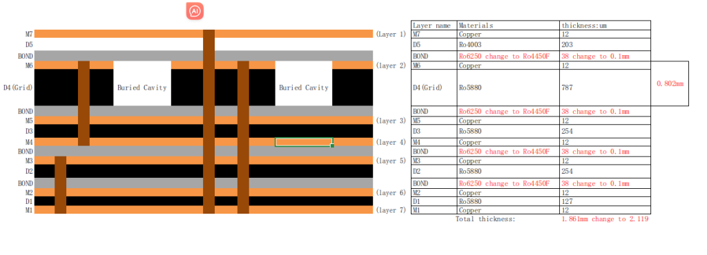
El proceso de fabricación de Sustrato de cavidad.
El proceso de fabricación de sustratos de cavidades requiere una serie de pasos precisos para garantizar un rendimiento estable y una calidad confiable del producto final.. A continuación se muestra una descripción detallada de cada paso.:
Diseño y Dibujo
En la etapa inicial de fabricación del sustrato de la cavidad., Los ingenieros utilizan software de diseño profesional para dibujar diagramas de circuitos y estructuras de cavidades.. Esta etapa requiere tener en cuenta los requisitos funcionales del circuito así como el tamaño y forma de la cavidad.. A través de software CAD, Los ingenieros pueden determinar con precisión el método de conexión del circuito y el diseño de la cavidad., Proporcionar una guía de diseño precisa para los pasos de fabricación posteriores..
Preparación de materiales
Una vez completado el diseño, El proceso de fabricación entra en la etapa de preparación del material.. Según los requisitos de diseño., Seleccione el material de sustrato adecuado y realice el tratamiento previo necesario.. Los materiales de sustrato comúnmente utilizados incluyen resina epoxi reforzada con fibra de vidrio FR-4 y materiales cerámicos.. La calidad y precisión de la preparación del material son fundamentales para el rendimiento y la estabilidad del producto final..
Transferencia de patrón
La transferencia de patrones es un paso crítico en la transferencia de patrones de circuitos a la superficie del sustrato.. Esto generalmente se logra mediante técnicas de fotolitografía o serigrafía.. en este proceso, Se aplica fotorresistente o tinta a la superficie de un sustrato., y luego se utiliza una plantilla o máscara para transferir el patrón al sustrato. La precisión de la transferencia de patrones afecta directamente la precisión y eficiencia de los pasos posteriores..
Aguafuerte
El grabado es el paso de eliminar el exceso de material conductor para formar el patrón de circuito deseado.. Esto generalmente se logra mediante grabado químico o procesamiento mecánico.. En grabado químico, El sustrato se sumerge en una solución corrosiva que disuelve las partes del material conductor que no están cubiertas por fotoprotector o tinta.. en mecanizado, Se utiliza equipo de procesamiento de precisión para eliminar el exceso de material.. El control preciso y la alta eficiencia del proceso de grabado son clave para garantizar la calidad y la estabilidad del circuito..
Perforación y revestimiento
Una vez completado el grabado, Es necesario perforar agujeros en el sustrato y realizar una galvanoplastia para conectar los circuitos multicapa.. El proceso de perforación requiere equipos de perforación de alta precisión para garantizar la exactitud del diámetro y la ubicación del orificio.. El proceso de galvanoplastia consiste en recubrir una capa de material conductor en la pared del orificio para facilitar las conexiones posteriores entre las capas del circuito..
Procesamiento de cavidades
El procesamiento de cavidades consiste en formar una estructura de cavidad para acomodar componentes electrónicos y lograr una mayor integración.. Esto generalmente se logra mediante técnicas de corte por láser o mecanizado.. Según los requisitos de diseño., Los ingenieros cortan o procesan con precisión el sustrato para formar la estructura de cavidad requerida..
Montaje y prueba
El último paso es montar los componentes electrónicos en el sustrato de la cavidad y realizar pruebas funcionales e inspecciones de calidad.. Durante el proceso de montaje, Los ingenieros necesitan instalar con precisión varios componentes y soldarlos o conectarlos de acuerdo con los requisitos de diseño.. Después de completar el montaje, Realizar pruebas funcionales para garantizar el funcionamiento normal del circuito.. Al mismo tiempo, Se llevan a cabo inspecciones de calidad para garantizar que los productos cumplan con las normas y regulaciones pertinentes..
El área de aplicación del sustrato de cavidades.
El sustrato de cavidad es una tecnología clave ampliamente utilizada en dispositivos electrónicos. Su excelente rendimiento y diseño flexible lo hacen desempeñar un papel importante en muchos campos..
Equipos de comunicación inalámbrica.
En el campo de los equipos de comunicación inalámbrica., como teléfonos móviles, enrutadores, etc., Los sustratos de cavidades se utilizan ampliamente.. Debido a la creciente demanda de rendimiento de alta frecuencia y diseños compactos en estos dispositivos, Los sustratos de cavidad pueden proporcionar un excelente rendimiento de transmisión de señal al tiempo que permiten diseños de circuitos compactos.. Instalando y empaquetando componentes clave dentro de la cavidad, La interferencia de la señal se puede reducir eficazmente y mejorar la calidad y estabilidad de la comunicación..
Equipo medico
En el campo de los dispositivos médicos., Los sustratos de las cavidades desempeñan un papel clave en los dispositivos médicos implantables.. Los dispositivos médicos implantables tienen requisitos extremadamente altos en cuanto a confiabilidad y miniaturización del dispositivo., y los sustratos de cavidades pueden satisfacer estas necesidades. Al adoptar una estructura de cavidad, Los componentes electrónicos se pueden integrar de forma compacta dentro del dispositivo médico y al mismo tiempo proporcionan buenos efectos de protección y aislamiento para garantizar que el dispositivo funcione de manera estable y confiable en el entorno in vivo..
Electrónica del vehículo
En el campo de la electrónica del automóvil., Los sustratos de cavidad se utilizan ampliamente en sistemas de control de automóviles y módulos de sensores.. Los equipos electrónicos automotrices requieren resistencia a altas temperaturas y alta confiabilidad., y los sustratos de cavidades pueden proporcionar una excelente resistencia al calor y estabilidad estructural. Instalando y encapsulando componentes electrónicos clave dentro de la cavidad, Se pueden proteger eficazmente de factores ambientales como la vibración del vehículo., humedad, y alta temperatura, asegurando así un funcionamiento estable a largo plazo de los equipos electrónicos automotrices.
Aeroespacial
En el campo aeroespacial, Los sustratos de cavidades se utilizan ampliamente en satélites y naves espaciales.. Los equipos aeroespaciales tienen requisitos extremadamente altos para una alta durabilidad y estabilidad del equipo., y los sustratos de cavidades pueden proporcionar una excelente estabilidad estructural y rendimiento eléctrico.. Instalando y encapsulando componentes electrónicos clave dentro de la cavidad, Puede protegerlo eficazmente de los efectos ambientales extremos durante el lanzamiento de la nave espacial., garantizando al mismo tiempo su funcionamiento fiable a largo plazo en el espacio.
Para resumir, Los sustratos de cavidad juegan un papel importante e irremplazable en los campos de las comunicaciones inalámbricas., atención médica, automóviles, aeroespacial y otros campos, proporcionando soporte clave para la mejora del rendimiento y la innovación de los dispositivos electrónicos. Con el continuo avance de la tecnología y la continua expansión de los campos de aplicación., Los sustratos de las cavidades seguirán desempeñando un papel cada vez más importante..
¿Cuáles son las ventajas del sustrato de cavidades??
Como tipo especial de PCB, El sustrato de cavidad muestra ventajas únicas en los equipos electrónicos modernos.. Sus principales ventajas incluyen:
Alta integración
Una característica especial del diseño del sustrato de la cavidad es el área rebajada dentro o sobre su superficie., que proporciona espacio adicional para el montaje de componentes electrónicos. Esto significa que se pueden acomodar más componentes dentro de un tamaño físico relativamente pequeño., permitiendo un mayor nivel de integración. Esta ventaja es particularmente significativa para aplicaciones con volumen limitado., como dispositivos móviles o drones.
Excelentes propiedades eléctricas
El diseño del sustrato de la cavidad puede reducir eficazmente la pérdida de señal y la interferencia electromagnética.. Porque el espacio entre componentes es menor y las rutas de transmisión de señales son más cortas, La estabilidad y el rendimiento del circuito son más fiables.. Especialmente en circuitos de alta frecuencia y RF., La integridad de la señal es crítica para el rendimiento del sistema., y los sustratos de cavidad pueden proporcionar un entorno de transmisión de señal más confiable.
Mejor gestión térmica
El diseño optimizado de la cavidad puede mejorar eficazmente el efecto de disipación de calor.. En equipos electrónicos de alta densidad de potencia., como servidores o amplificadores de potencia, La gestión térmica es fundamental.. Los sustratos de cavidad ayudan a conducir y disipar eficientemente el calor lejos de los componentes al proporcionar una superficie más grande para la disipación del calor y una mejor circulación del aire., manteniendo así la estabilidad y confiabilidad del sistema.
Alta resistencia mecánica
El diseño estructural del sustrato de la cavidad le confiere mayor resistencia mecánica y durabilidad.. En comparación con el single tradicional- o PCB de doble capa, Los sustratos de cavidades suelen tener una estructura más fuerte y pueden soportar mayores tensiones mecánicas y vibraciones.. Esta propiedad hace que los sustratos de cavidades sean particularmente adecuados para aplicaciones que operan en condiciones ambientales adversas., como electrónica automotriz o equipos aeroespaciales.
En resumen, Los sustratos de cavidad proporcionan un importante soporte técnico y espacio de desarrollo para el diseño y fabricación de dispositivos electrónicos modernos a través de su alta integración., excelentes propiedades eléctricas, buena gestión térmica, y excelente resistencia mecánica. A medida que los requisitos de rendimiento y volumen de los productos electrónicos continúan aumentando, La tecnología de sustrato de cavidad desempeñará un papel importante en más campos y llevará la industria electrónica a un nivel superior..
Preguntas frecuentes
¿Cuál es el costo del sustrato de la cavidad??
El coste del sustrato de la cavidad es ligeramente superior al de la placa de circuito impreso tradicional. (tarjeta de circuito impreso). Esto se debe principalmente a que el proceso de diseño y fabricación del sustrato de la cavidad requiere más procesos y equipos de precisión.. Sin embargo, el costo es aceptable dadas las ventajas de rendimiento que pueden proporcionar los sustratos de cavidades, especialmente en aplicaciones de circuitos de RF y alta frecuencia. En algunos campos con mayores requisitos de rendimiento, como las comunicaciones, campos médicos y militares, Las ventajas de rendimiento del sustrato de cavidad a menudo pueden compensar su costo ligeramente mayor., por lo que tiene una buena relación precio/rendimiento.
¿Se pueden utilizar sustratos de cavidad en circuitos de alta frecuencia??
Sí, Los sustratos de cavidad son particularmente adecuados para circuitos de alta frecuencia y RF.. Dado que el área rebajada dentro o en la superficie del sustrato de la cavidad puede reducir efectivamente la ruta de transmisión de la señal., reducir la pérdida de señal y la interferencia, Puede mejorar significativamente el rendimiento y la estabilidad de los circuitos de alta frecuencia.. Esto hace que los sustratos de cavidad sean ideales para su uso en comunicaciones inalámbricas., sistemas de radar, Comunicaciones por satélite, y más.
¿Es difícil procesar el sustrato de la cavidad??
Los requisitos de procesamiento del sustrato de la cavidad son altos y requieren equipos y procesos de fabricación precisos.. Especialmente en el procesamiento de estructuras huecas., Generalmente se requiere tecnología avanzada de corte por láser o mecanizado de precisión para garantizar que el tamaño y la forma de la cavidad cumplan con los requisitos de diseño.. Sin embargo, con el avance continuo de la tecnología de fabricación, la dificultad de procesamiento se reduce gradualmente, y la eficiencia de producción y la precisión del procesamiento también mejoran constantemente. Por lo tanto, aunque el procesamiento de sustratos de cavidades es relativamente complejo, Aún se puede lograr una producción de alta calidad con el apoyo de fabricantes profesionales..