CO., LTD")
Cerámico sustrato del paquete Fabricante, Proveedor de placa de circuito cerámico y sustratos de paquete cerámico BGA. Ofrecemos PCB cerámicos HDI microtrace/microgap y sustratos BGA cerámicos de 1 capa a 30 capas.
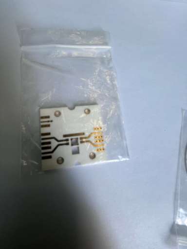
Los sustratos de paquetes cerámicos son componentes vitales en la electrónica moderna, brindando apoyo, conexión, y protección para chips y otros elementos electrónicos. Hecho de materiales como óxido de aluminio. (Alúmina) o nitruro de aluminio (Nitruro de aluminio), Ofrecen una conductividad eléctrica y térmica excepcional., superando a los materiales tradicionales por su resistencia a las altas temperaturas, corrosión, y resistencia mecánica. Estos sustratos sirven como plataformas resistentes para soportar e interconectar componentes electrónicos., Empleando cableado de alta densidad y técnicas de soldadura precisas para garantizar la integridad y confiabilidad del circuito.. Sus capacidades superiores de disipación de calor los hacen ideales para dispositivos electrónicos de alta potencia., Mejorar el rendimiento y la confiabilidad del equipo en diversos entornos..
En resumen, El sustrato de paquete cerámico se erige como una tecnología fundamental de embalaje electrónico con excelentes propiedades físicas y eléctricas.. Desempeña un papel crucial en varios sistemas de alto rendimiento., dispositivos electrónicos de alta densidad, ofreciendo un soporte sólido, conexiones confiables, y adaptabilidad a diversas condiciones ambientales. Esta tecnología abre nuevas posibilidades y oportunidades en el ámbito de la ingeniería electrónica.
¿Qué tipos de Sustrato Paquete Cerámico existen??
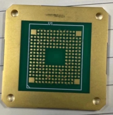
Los sustratos de paquete cerámico son cruciales tarjeta de circuito impreso Tecnología que ofrece varios tipos adaptados a diferentes aplicaciones y requisitos de diseño., incluyendo notablemente BGA (Matriz de rejilla de bolas) y CSP (Paquete de báscula de chips). BGA, caracterizado por una serie de bolas de soldadura debajo del chip para conectarse a las almohadillas en la PCB, permite empaquetar chips de alta densidad con excelente rendimiento eléctrico y capacidades de gestión térmica. Su diseño uniforme y confiable de la bola de soldadura hace que se utilice ampliamente en computadoras de alto rendimiento., equipo de comunicacion, sistemas de control industriales, y otras áreas que requieren alta integración y confiabilidad.
Otro tipo común de sustrato cerámico es el CSP. (Paquete de báscula de chips), que minimiza el tamaño del chip en el paquete y lo conecta directamente a la PCB en la parte inferior del paquete sin requerir pines o conectores adicionales. Este diseño permite a CSP lograr paquetes más pequeños, ahorrando así espacio y mejorando la integración del sistema. CSP se usa comúnmente en dispositivos móviles, electrónica de consumo, y sistemas integrados donde los requisitos de tamaño y peso son más estrictos y al mismo tiempo mantienen un buen rendimiento y confiabilidad..
Los sustratos de paquetes cerámicos ofrecen soluciones versátiles adaptadas a diversos escenarios de aplicación y requisitos de diseño.. Ya sea para informática de alto rendimiento o dispositivos móviles compactos, Los sustratos cerámicos satisfacen hábilmente las necesidades de diseño de diversos dispositivos electrónicos., asegurando una base estable y confiable.
¿Cuáles son las ventajas del sustrato de paquete cerámico??
El sustrato cerámico ofrece ventajas significativas sobre las placas de circuitos tradicionales.. En primer lugar, su confiabilidad y estabilidad son inigualables debido a su composición de materiales cerámicos, proporcionando una excelente resistencia a altas temperaturas y estabilidad química, Garantizar el funcionamiento prolongado del equipo en condiciones extremas..
El sustrato cerámico ofrece soluciones de diseño compactas y duraderas, atendiendo a la demanda de elegante, dispositivos electrónicos ligeros. Su alta resistencia y dureza permiten diseños más pequeños en comparación con los tableros tradicionales.. Además, cuenta con capacidades superiores de disipación de calor, Dispersar eficientemente el calor para mejorar la estabilidad del sistema.. A través de técnicas de fabricación avanzadas, Permite mayores niveles de integración., Reducir las distancias de interconexión y mejorar el rendimiento de los circuitos.. A pesar de los desafíos iniciales, Los avances tecnológicos han hecho que los sustratos cerámicos sean rentables para la producción a gran escala., convirtiéndolos en una opción vital en el diseño de equipos electrónicos modernos.
¿Por qué elegir el sustrato cerámico??
Al considerar las opciones de placas de circuito, El sustrato cerámico se destaca por sus ventajas únicas y su idoneidad para dispositivos electrónicos de alto rendimiento.. Su preferencia se debe a su capacidad para ofrecer un rendimiento superior en comparación con otros tipos de placas de circuito..
Los sustratos cerámicos en paquete son muy valorados por su excepcional confiabilidad., convirtiéndolos en la opción preferida en sectores críticos como el aeroespacial, médico, y aplicaciones militares. Su estabilidad superior da como resultado menos fallas en los circuitos., Garantizar que el equipo funcione de manera confiable a largo plazo..
Además, Los sustratos cerámicos en paquete cuentan con una notable resistencia a las altas temperaturas., un atributo crucial para entornos exigentes. Sus propiedades cerámicas innatas permiten un rendimiento constante incluso en condiciones extremas., haciéndolos ideales para altas temperaturas, alta frecuencia, o dispositivos electrónicos de alta potencia como sistemas de comunicación por microondas y computadoras de alto rendimiento.
Además, Estos sustratos demuestran un rendimiento eléctrico excepcional.. Sus excelentes propiedades dieléctricas y conductividad térmica reducen eficazmente la pérdida de señal y la acumulación de calor., mejorando el rendimiento y la estabilidad general del circuito. Como consecuencia, Los sustratos de paquete cerámico son la opción preferida para implementar dispositivos electrónicos más rápidos y de mayor rendimiento..
En resumen, la combinación de una fiabilidad excepcional, alta resistencia a la temperatura, y sus excelentes capacidades eléctricas posicionan a los sustratos cerámicos como la opción preferida para dispositivos electrónicos de alto rendimiento.. En esfuerzos de ingeniería electrónica que enfatizan la estabilidad., fiabilidad, y rendimiento superior, Optar por sustratos cerámicos en paquete establece una base confiable para el éxito del proyecto y la excelencia operativa a largo plazo..
¿Cuál es el proceso de fabricación del Sustrato Paquete Cerámico??
El proceso de fabricación de Sustratos Paquetes Cerámicos es un procedimiento complejo y preciso que involucra varios pasos meticulosos y el uso de tecnologías avanzadas.. Inicialmente, La fase de diseño es crucial., donde se emplea software CAD para determinar el diseño del circuito, posicionamiento de componentes, y esquemas de conectividad, considerando factores como el tamaño y las características térmicas/eléctricas.
Los materiales clave necesarios incluyen sustratos cerámicos., alambres metálicos, y materiales de embalaje, todo sujeto a rigurosos controles y pruebas para garantizar el cumplimiento de la calidad.. El proceso comienza recubriendo el sustrato cerámico con una capa conductora y usando fotolitografía para formar patrones de circuito en la placa base o PCB..
Próximo, la PCB se apila con otras capas, incluyendo alambres de metal, materiales aislantes, y capas cerámicas adicionales, que se consolidan mediante laminación a alta temperatura y presión.. Se añaden capas de metalización para facilitar la conectividad entre dispositivos electrónicos, logrado a través de procesos como el grabado químico o la evaporación del metal.
Después de la metalización y laminación., la PCB se somete a moldeo y encapsulación, donde los componentes electrónicos se montan y encapsulan con materiales protectores para protegerlos de elementos externos. Siguen las pruebas finales y el control de calidad., que abarca inspecciones integrales del rendimiento eléctrico, tamaño, apariencia, y confiabilidad para garantizar el cumplimiento de las especificaciones de diseño y los estándares de calidad.
En resumen, El proceso de fabricación del sustrato cerámico implica una artesanía compleja y tecnología avanzada para ofrecer alta calidad., Sustratos de alto rendimiento esenciales para respaldar la evolución de los dispositivos electrónicos..
¿En qué campos se utiliza el Sustrato Paquete Cerámico??
Ceramic Package Substrate aborda este desafío al permitir una mayor integración y factores de forma compactos., ofreciendo una mayor flexibilidad de diseño para dispositivos móviles. Sus capacidades superiores de disipación de calor también contribuyen a mantener un rendimiento estable y prolongar la vida útil del teléfono inteligente..
Similarmente, en ordenadores y servidores de alto rendimiento, El sustrato de paquete cerámico se utiliza ampliamente para satisfacer las demandas de manejo de volúmenes de datos sustanciales y tareas informáticas complejas.. Con su rendimiento eléctrico estable y su excepcional disipación de calor, El sustrato cerámico garantiza un funcionamiento ininterrumpido y mejora el rendimiento general del sistema..
En el ámbito de los equipos de comunicación., El sustrato cerámico en paquete también tiene importancia. Ya sea equipo de estación base, infraestructura de red, o módulos de comunicación, Las placas de circuito robustas son imprescindibles para soportar sus funciones multifacéticas y tareas de comunicación.. La alta integración y estabilidad que ofrece Ceramic Package Substrate lo convierten en la opción preferida para este tipo de equipos., reforzando eficazmente su rendimiento y confiabilidad.
En resumen, Ceramic Package Substrate exhibe un rendimiento de aplicación ejemplar en teléfonos inteligentes, computadoras, equipo de comunicacion, y más allá. Sus destacadas características proporcionan un soporte crucial para el diseño y fabricación de diversos dispositivos electrónicos., impulsando así avances y progreso dentro de la industria electrónica.
Cómo encontrar sustrato de paquete cerámico?
Seleccionar el sustrato cerámico adecuado es vital para garantizar la eficacia y confiabilidad de los dispositivos electrónicos.. Al buscar proveedores y fabricantes, elegir el socio adecuado es primordial. nuestra empresa, dedicados a ofrecer materiales electrónicos premium, está totalmente comprometido a brindarle soporte y servicios integrales.
El proceso de encontrar el sustrato cerámico ideal implica varias vías. En primer lugar, Puede utilizar recursos en línea para investigar diferentes tipos de productos y especificaciones disponibles en el mercado.. En segundo lugar, Llegar a proveedores profesionales de material electrónico., que normalmente ofrecen una gama de soluciones de selección y personalización para sustratos de paquetes cerámicos., es aconsejable.
Como proveedor profesional de materiales electrónicos., Nuestra empresa se dedica a ofrecer productos y servicios de sustrato cerámico de primer nivel.. Con nuestra amplia experiencia y equipo capacitado, Ofrecemos soluciones a medida basadas en los requisitos del cliente.. Colaborar con fabricantes reconocidos a nivel mundial garantiza la confiabilidad y el cumplimiento de los estándares y especificaciones de la industria de nuestros productos.. Ya sea que necesite especificaciones estándar o soluciones personalizadas, Podemos satisfacer sus necesidades y brindarle soporte y servicios técnicos expertos..
como tu pareja, nuestra empresa ofrece los siguientes beneficios:
Equipo profesional: Contamos con un equipo técnico experto capaz de brindar consultas expertas y asistencia técnica..
Our company ensures the provision of high-quality Ceramic Package Substrate products through collaboration with internationally renowned manufacturers, guaranteeing reliability and superior performance. We offer customized solutions tailored to meet specific customer requirements for various application scenarios. With a steadfast commitment to punctual delivery, we prioritize meeting customer needs promptly. Whether seeking standard specifications or personalized solutions, our team is dedicated to providing professional support and services, partnering with clients to forge a brighter future together.
¿Cuál es la cotización del sustrato cerámico en paquete??
Obtaining a quote for Ceramic Package Substrate is a crucial step that directly impacts project cost and feasibility. In the following discussion, we’ll explore the process of obtaining these quotes and how market pricing, along with other factors, influences them.
Primero, the most direct way to get a quote for Ceramic Package Substrate is to contact the manufacturer or supplier. Típicamente, these companies provide online quoting tools or communicate with customers via email, teléfono, etc.. By providing detailed specification requirements and quantity requirements, customers can obtain accurate quotation information.
Apart from market forces, Ceramic Package Substrate quotations are also influenced by specific requirements. Factores como el tamaño, recuento de capas, and material type impact manufacturing costs, thereby affecting the final quotation. Larger order quantities generally result in lower unit prices due to economies of scale, while smaller batches may incur higher unit costs.
The specified delivery time plays a crucial role, with manufacturers potentially imposing extra charges for expedited delivery or urgent order processing, thereby affecting the overall quotation. Additional services such as sample testing or custom design may also be available, impacting the final cost.
En resumen, obtaining a quotation for Ceramic Package Substrate involves not only considering market-related factors but also specific specification requirements, cantidad de pedido, el tiempo de entrega, and potential additional services. By taking these factors into account, customers can secure a quote that aligns with their needs and budget, facilitating informed decision-making.
¿Cuáles son las preguntas frecuentes sobre el Sustrato Paquete Cerámico??
¿Qué distingue al sustrato cerámico del paquete de PCB tradicionales??
Ceramic Package Substrate differs significantly from traditional PCBs. Its composition, propiedades térmicas, and application areas set it apart. Understanding these distinctions is key to appreciating its advantages.
¿Qué tipos de dispositivos electrónicos se benefician más del sustrato cerámico en paquete??
While Ceramic Package Substrate finds applications across various electronic devices, understanding which devices benefit the most is essential. From smartphones to communication equipment, delving into specific use cases provides valuable insights.
¿De qué manera el sustrato cerámico impacta las consideraciones de costos en el desarrollo de dispositivos electrónicos??
Cost is a significant factor in any technology adoption. Examining how Ceramic Package Substrate influences overall project costs assists in making informed decisions during the design and development phases.
¿Cuáles son las ventajas clave del sustrato cerámico en términos de confiabilidad y resistencia a la temperatura??
Reliability and temperature resistance are critical factors in electronic components. Exploring how Ceramic Package Substrate excels in these aspects sheds light on its suitability for high-performance applications and harsh operating conditions.
¿Cómo se determinan las cotizaciones de sustratos cerámicos??
Ceramic Package Substrate quotes depend on factors such as substrate material, complejidad, volumen de producción, y requisitos de personalización. Request quotes from trusted suppliers to ensure accurate cost estimation for your project.