CO., LTD")
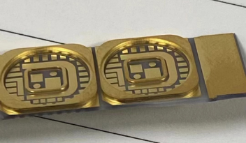
Cavidad incrustada tarjeta de circuito impreso Fabricante de sustratos. Cavidad de material de alta velocidad y alta frecuencia sustrato de embalaje y fabricación de PCB con ranura de cavidad.
El sustrato PCB de cavidad integrada representa una innovación revolucionaria en el campo de la electrónica, impulsando el desarrollo de placas de circuitos a alturas sin precedentes. En su núcleo, este sustrato se distingue por la incorporación de una estructura de cavidad incrustada, una característica que va más allá de la mera estética para abordar las demandas de los dispositivos electrónicos contemporáneos para una mejor integración y miniaturización.. La inclusión estratégica de cavidades dentro del diseño de la placa de circuito facilita la realización de diseños de circuitos más complejos y compactos., En última instancia, contribuye a un mayor rendimiento y confiabilidad en los dispositivos electrónicos..
Mayor integración: El diseño de la cavidad integrada permite que los componentes del circuito se dispongan más juntos en un espacio limitado., logrando así un mayor nivel de integración. Esto significa que se pueden incluir más funciones y rendimiento en un espacio relativamente pequeño., dando al dispositivo más flexibilidad de diseño.
tamaño más pequeño: El diseño del sustrato de PCB con cavidad integrada permite reducir el tamaño total del dispositivo. Esto es fundamental para los dispositivos electrónicos de consumo modernos, ya que los usuarios esperan que sean más livianos., más productos portátiles.
Excelente capacidad de disipación de calor: La compacidad mejorada de los componentes del circuito va acompañada de una cavidad integrada meticulosamente diseñada., aumentando significativamente la eficiencia de disipación de calor. Esto se vuelve fundamental para la funcionalidad sostenida de alto rendimiento de los dispositivos electrónicos., Garantizar la confiabilidad del equipo en diversos escenarios de uso durante períodos prolongados..
Su aplicación en el campo de la ingeniería electrónica aporta nuevas posibilidades al diseño de equipos, y también hace que los productos electrónicos estén más en línea con los usuarios’ expectativas para los pequeños, equipos de alto rendimiento. La innovación de los sustratos de placas de circuitos con cavidades integradas seguirá liderando el desarrollo del campo electrónico y proporcionará un fuerte apoyo para la innovación tecnológica y el diseño de equipos en el futuro..
¿Qué tipos de sustrato de PCB con cavidad integrada existen??
En el rápido desarrollo del campo electrónico, El sustrato de PCB con cavidad integrada se está convirtiendo en el centro del diseño de circuitos, y sus diferentes tipos, como BGA (Matriz de rejilla de bolas) y CSP (Paquete de báscula de chips), etc., han demostrado ventajas únicas en aplicaciones prácticas.
BGA es una tecnología de empaquetamiento con matriz de rejilla de bolas caracterizada por una base llena de pequeños conectores de bolas que se conectan a almohadillas en una placa de circuito.. Este diseño tiene ventajas obvias en circuitos integrados de alta densidad.. Con distancias de conexión más cortas, Los BGA proporcionan una inductancia más baja y una mayor integridad de la señal, especialmente en aplicaciones de alta frecuencia.
El CSP es un paquete compacto que tiene casi el mismo tamaño que el propio chip.. Comparado con el embalaje tradicional, CSP proporciona un diseño de menor tamaño y peso más ligero, adecuado para las necesidades de dispositivos delgados y livianos. Sus características de baja inductancia y baja resistencia hacen que la transmisión de la señal sea más rápida y más amigable con la disipación del calor..
Integración y rendimiento: BGA y CSP, como tipos de sustrato de PCB con cavidad integrada, Ambos mejoran la integración del circuito a través de métodos de embalaje innovadores., optimizando así el rendimiento general.
Tamaño y peso: Debido a su diseño compacto, CSP hace que el dispositivo en general sea más delgado y liviano, haciéndolo adecuado para aplicaciones con requisitos estrictos de tamaño y peso.
Integridad de la señal: BGA proporciona distancias de conexión más cortas mediante conexiones de rejilla de bolas, reduciendo la inductancia y ayudando a mantener la integridad de la señal, especialmente adecuado para aplicaciones de alta frecuencia.
Rendimiento de disipación de calor: El tamaño compacto de CSP contribuye a una mejor disipación del calor., lo que lo convierte en una excelente opción para aplicaciones con requisitos térmicos exigentes.
Campos aplicables: BGA es ideal para escenarios que requieren diseños de alta densidad y rendimiento superior., mientras que CSP es más adecuado para dispositivos delgados y livianos como teléfonos inteligentes y dispositivos portátiles.
Al seleccionar el tipo de sustrato de PCB con cavidad integrada, Los diseñadores deben considerar cuidadosamente los requisitos específicos de la aplicación para elegir la tecnología de embalaje que mejor se alinee con los objetivos de diseño del dispositivo.. Ya sea priorizando el alto rendimiento, factor de forma pequeño, o disipación de calor excepcional, BGA y CSP ofrecen opciones flexibles, proporcionando un amplio espacio para el diseño innovador de dispositivos electrónicos.
¿Cuáles son las ventajas del sustrato de PCB con cavidad integrada??
En el diseño electrónico contemporáneo, El sustrato de PCB con cavidad integrada está ganando cada vez más popularidad debido a su diseño distintivo y ventajas de rendimiento avanzadas., lo que lo convierte en una opción óptima para equipos electrónicos de alta gama. A diferencia de las placas de circuito tradicionales, El sustrato de PCB con cavidad integrada ofrece varias ventajas únicas.
Una ventaja clave radica en sus capacidades de integración avanzadas., permitiendo el alojamiento de numerosos componentes y funciones dentro de un espacio más pequeño. Integrando cavidades en PCB, Los elementos del circuito se pueden organizar más densamente., tanto vertical como horizontalmente. Esto permite el desarrollo de diseños de circuitos más complejos y altamente integrados..
Además, en comparación con las placas de circuitos tradicionales, El diseño de sustratos de PCB con cavidad integrada conduce a una reducción del tamaño y peso total.. Este diseño liviano es particularmente significativo en el ámbito de los dispositivos electrónicos livianos., como dispositivos portátiles y drones, contribuyendo a mejorar la portabilidad y maniobrabilidad de los dispositivos.
El diseño de la cavidad integrada ayuda a mejorar el rendimiento de disipación de calor.. Dejando espacio en la PCB, El calor se puede conducir y disipar más fácilmente., ralentizar eficazmente el aumento de temperatura del dispositivo durante el funcionamiento con carga alta.
El sustrato de PCB con cavidad integrada está diseñado específicamente para mitigar la diafonía y la distorsión de la señal durante la transmisión de la señal.. Mediante la incorporación de una cavidad incrustada dentro de la PCB, Las líneas de señal experimentan un aislamiento mejorado, lo que conduce a una mejor integridad de la señal y garantiza la transmisión confiable de datos.
La creciente necesidad de dispositivos electrónicos avanzados con capacidades de alta frecuencia ha dado lugar a los sustratos de PCB con cavidades integradas.. Estos sustratos proporcionan una gestión precisa de las rutas de propagación de la señal y la impedancia., haciéndolos muy adecuados para manejar señales de alta frecuencia, especialmente en circuitos de RF y microondas.
El diseño innovador de las cavidades integradas proporciona un espacio de diseño más flexible., Permitir a los diseñadores organizar componentes y cableado con mayor libertad.. Esta adaptabilidad hace que los sustratos de PCB con cavidad integrada sean una opción versátil para diseños de dispositivos electrónicos complejos y exigentes., proporcionando un amplio espacio para la innovación.
El sustrato de PCB con cavidad integrada surge como una opción superior para diseños de dispositivos electrónicos de alta gama en comparación con las placas de circuitos convencionales.. Este avanzado sustrato de PCB no solo cumple con las rigurosas demandas de los equipos electrónicos contemporáneos en términos de rendimiento y confiabilidad, sino que también actúa como una plataforma sólida para la innovación continua en el ámbito de la ingeniería electrónica..
¿Por qué elegir el sustrato de PCB con cavidad integrada??
En primer lugar, la ventaja de tamaño del sustrato de PCB con cavidad integrada es obvia. Debido a su diseño de cavidad integrada, este tipo de placa permite un mayor nivel de integración de circuitos, reduciendo así el tamaño total del dispositivo. Este diseño compacto es una ventaja importante para los dispositivos electrónicos cada vez más miniaturizados de hoy en día., Proporcionar a los diseñadores una mayor flexibilidad para que los dispositivos puedan caber más fácilmente en limitaciones de espacio complejas..
En segundo lugar, El sustrato de PCB con cavidad integrada demuestra un rendimiento excepcional de disipación de calor. La estructura de la cavidad no solo mejora la ventilación del circuito sino que también permite una disipación eficiente del calor.. En equipos de alto rendimiento, La disipación de calor efectiva es esencial para mantener un funcionamiento estable y extender la vida útil del equipo.. En comparación con las placas de circuito tradicionales, La capacidad superior de disipación de calor del sustrato de PCB con cavidad integrada mejora la confiabilidad en entornos exigentes., entornos de trabajo de alta carga.
Además, El proceso de fabricación del sustrato de PCB con cavidad integrada se ha vuelto cada vez más refinado., lo que resulta en un costo de producción relativamente estable. A medida que la tecnología continúa avanzando, Los fabricantes han implementado numerosas mejoras en el proceso de fabricación de placas de circuitos con cavidades integradas., lo que lleva a reducciones de costos en la producción. Esto permite a los diseñadores ejercer un control más efectivo sobre el costo general del proyecto mientras se esfuerzan por lograr un alto rendimiento., mejorando así la competitividad general del sustrato de PCB con cavidad integrada.
Además, Este tipo de placa de circuito también tiene ventajas únicas en la transmisión de señales eléctricas.. El diseño de cavidad integrada reduce la interferencia electromagnética en la transmisión de señales y mejora la integridad general de la señal.. Esto es particularmente importante para algunas aplicaciones que requieren una calidad de señal extremadamente alta., como equipos de comunicación de alta frecuencia.
En general, Los diseñadores eligen el sustrato de PCB con cavidad integrada principalmente debido a sus amplias ventajas en tamaño., disipación de calor, Costo e integridad de la señal.. A medida que los dispositivos electrónicos continúan buscando rendimiento y tamaño,
¿En qué campos de aplicación se utiliza ampliamente el sustrato de PCB con cavidad integrada??
En el ámbito de las industrias contemporáneas de alta tecnología, El sustrato de PCB con cavidad integrada desempeña un papel fundamental en el panorama del diseño de productos electrónicos., que abarca dispositivos como teléfonos inteligentes, computadoras, y equipos de comunicación. Su uso extensivo no sólo mejora el rendimiento general de los dispositivos electrónicos sino que también establece una base sólida para la implementación de funcionalidades y tecnologías avanzadas..
Dado que los teléfonos inteligentes tienen requisitos extremadamente altos en cuanto a tamaño y rendimiento, La alta integración y el diseño compacto del sustrato de PCB con cavidad integrada permiten que los teléfonos móviles sean más delgados y livianos y acomoden componentes más avanzados.. Este diseño no sólo ayuda a aumentar la velocidad de procesamiento, pero también admite funciones multimedia y de comunicación más complejas, proporcionando a los usuarios una experiencia más rica.
El sustrato de PCB con cavidad integrada se presenta como una solución óptima en el campo de la tecnología informática., permitiendo el diseño de computadoras de alto rendimiento y sistemas integrados. Su diseño compacto permite una mayor integración de componentes electrónicos en un espacio más pequeño., aumentando así la potencia informática y las velocidades de transferencia de datos. Este diseño innovador sirve como base para avances en el procesamiento de grandes conjuntos de datos., inteligencia artificial, y aplicaciones gráficas complejas.
En la fabricación de equipos de comunicación., El sustrato de PCB con cavidad integrada juega un papel crucial. La incorporación de una cavidad en la placa de circuito mejora la eficiencia de transmisión de la señal al tiempo que minimiza el riesgo de interferencia de la señal.. Esta característica es esencial para garantizar la confiabilidad de los equipos de comunicación., particularmente en el soporte de tecnologías de comunicación avanzadas, como la transmisión de datos de alta velocidad, redes celulares, y comunicaciones satelitales.
Los fabricantes de dispositivos pueden integrar sin problemas varios sensores, papas fritas, y componentes, permitiendo la realización de funciones más complejas e inteligentes. Los ejemplos incluyen los importantes beneficios de las tecnologías avanzadas como el reconocimiento facial., realidad virtual, y realidad aumentada, todo lo cual prospera gracias al alto nivel de integración que ofrece el sustrato de PCB con cavidad integrada.
En resumen, la aplicación generalizada de sustratos de placas de circuitos con cavidades integradas en teléfonos inteligentes, computadoras, y los equipos de comunicación no solo mejoran el rendimiento del dispositivo sino que también establecen una base sólida para fomentar la innovación en la tecnología electrónica. Su contribución al soporte de funciones y tecnologías avanzadas lo convierte en un componente indispensable y crítico en el diseño de productos de alta tecnología contemporáneos..
Cómo encontrar un fabricante de sustrato de PCB con cavidad integrada?
En el panorama en rápida evolución de la industria electrónica, Se ha vuelto imperativo identificar un fabricante confiable de sustratos de PCB con cavidad integrada.. Optar por un fabricante con amplia experiencia y una reputación estelar es fundamental para garantizar la calidad y confiabilidad de sus equipos electrónicos.. Para navegar este proceso de manera efectiva, considere las siguientes sugerencias y pasos cuando busque un fabricante de sustrato de PCB con cavidad integrada.
Ante todo, Hay varias vías para descubrir fabricantes en este nicho., y un enfoque eficaz es participar en ferias y eventos relevantes de la industria.. Estos encuentros sirven de nexo entre profesionales de la industria y fabricantes., ofreciendo una plataforma directa para la comunicación. Al asistir a tales exposiciones, usted puede familiarizarse personalmente con los productos, tecnologías, y servicios de diferentes fabricantes, establecer conexiones iniciales con ellos.
Puede encontrar información sobre muchos proveedores a través de motores de búsqueda o plataformas profesionales de la industria electrónica.. Los foros en línea y las redes sociales también son una forma útil de obtener actualizaciones de la industria e información del fabricante.. En estas plataformas, Puede ver comentarios y reseñas de otros clientes para tener una idea de la reputación del fabricante y la satisfacción del cliente..
Sin embargo, Elegir un fabricante de sustrato de PCB con cavidad integrada no se trata solo de obtener información, también requiere una investigación más profunda. A continuación se ofrecen algunas sugerencias para asegurarse de elegir un fabricante con amplia experiencia y buena reputación.:
Reputación de marca: Revise la historia del fabricante y la reputación de la marca.. Descubra cuál es su posición en la industria y si han recibido certificaciones y premios relevantes..
Capacidades técnicas: Comprender la solidez técnica del fabricante y R.&capacidades D. Esto es esencial para garantizar que los productos sigan siendo tecnológicamente avanzados y se adapten a las necesidades cambiantes del mercado..
Comunicación y apoyo: Conéctese con fabricantes para conocer sus métodos de comunicación y sistemas de soporte.. La comunicación oportuna y un equipo de soporte sólido son clave para garantizar el éxito del proyecto..
En general, con una investigación exhaustiva y una investigación cuidadosa, puede tener más confianza al seleccionar un fabricante de sustrato de PCB con cavidad integrada que satisfaga sus necesidades. Nuestro equipo de relaciones con proveedores también ayudará activamente en el proceso de búsqueda de fabricantes para garantizar que reciba la mejor colaboración posible..
¿Dónde puedo obtener una cotización para el sustrato de PCB con cavidad integrada??
Para obtener una cotización precisa para el sustrato de PCB con cavidad integrada, debe tomar una serie de pasos específicos para conectarse con el fabricante y comprender los factores que intervienen en los servicios de fabricación personalizados..
Primero, establecer contacto con el fabricante es el primer paso para obtener un presupuesto detallado. Puedes comunicarte a través de:
Contacto por correo electrónico: Enviar requisitos de diseño detallados, presupuesto, cantidades, etc.. a la dirección de correo electrónico oficial del fabricante. Asegúrese de que su correo electrónico incluya suficientes detalles para que el fabricante comprenda exactamente lo que necesita..
comunicación telefónica: Hable directamente con el equipo de ventas del fabricante o representante profesional.. Esto ayuda a proporcionar información más directa., respuestas en tiempo real a las preguntas que pueda tener y garantiza que sus necesidades se comprendan completamente.
Al contactar con el fabricante, comprenda que los siguientes factores pueden afectar el precio de los servicios de fabricación personalizados del sustrato de PCB con cavidad integrada:
Requisitos de diseño: Si sus especificaciones de diseño son únicas o complejas, pueden necesitar aportes adicionales de ingenieros y técnicos, impactando los costos de fabricación.
Costo de material: Varios materiales de PCB tienen costos distintos, y la selección del material adecuado puede influir directamente en el coste total.
Proceso de fabricación: Los diseños especiales de cavidades integradas pueden requerir procesos de fabricación más complejos, potencialmente conduciendo a mayores costos de fabricación.
Cantidad de producción: La cantidad de producción generalmente afecta el precio unitario., por lo que es fundamental especificar el volumen de pedido esperado para obtener una cotización precisa.
El tiempo de entrega: Si tiene requisitos estrictos de tiempo de entrega, Se pueden incurrir en costos adicionales para garantizar una producción acelerada..
Estándares de calidad: Los requisitos de calidad especiales pueden exigir procesos de producción más rigurosos., influyendo en el coste total.
Al comunicarse con el fabricante., transmitir claramente estos factores para permitirles proporcionar una cotización más precisa. Además, solicitar cotizaciones para diferentes cantidades y condiciones de tiempo de entrega para facilitar una mejor planificación y toma de decisiones.
En general, con comunicación proactiva y una buena comprensión de los factores involucrados, Podrá obtener una cotización precisa para el sustrato de PCB con cavidad integrada que satisfaga sus necesidades..
¿Cuáles son los problemas comunes con el sustrato de PCB con cavidad integrada??
¿Qué ventajas ofrece un sustrato de PCB con cavidad integrada??
En comparación con las placas de circuito tradicionales, un sustrato de PCB con cavidad integrada presenta distintas ventajas. Estos incluyen niveles más altos de integración., dimensiones reducidas, y capacidades superiores de disipación de calor. Explorar estos beneficios proporciona una idea de por qué es una opción ideal para diseños de dispositivos electrónicos de alta gama..
¿Por qué elegir un sustrato de PCB con cavidad integrada en lugar de otras placas??
La creciente preferencia por los sustratos de PCB con cavidad integrada se debe a sus ventajas únicas sobre otros tipos de placas de circuito.. Esta sección profundiza en las razones específicas por las que los diseñadores optan por sustratos de PCB con cavidad integrada en diversas aplicaciones..
¿Cómo es el proceso de fabricación de los sustratos de PCB con cavidades integradas??
Comprender el proceso de fabricación es crucial. Esto incluye pasos para los tableros principal e inferior., así como la utilización de procesos y tecnologías avanzadas. El diseño de la cavidad integrada permite diseños de circuitos más complejos y compactos., contribuyendo a la funcionalidad general del sustrato.
¿En qué áreas de aplicación se utiliza ampliamente el sustrato de PCB con cavidad integrada??
Explore las amplias aplicaciones de los sustratos de PCB con cavidades integradas en áreas como los teléfonos inteligentes, computadoras, y dispositivos de comunicación. Descubra cómo las funciones altamente integradas la convierten en la opción preferida, soportando funcionalidades y tecnologías avanzadas.