CO., LTD")
Fabricante de sustratos encapsulados FC-LGA. Como fabricante líder de sustratos encapsulados FC-LGA, Nos especializamos en producir sustratos de alta calidad diseñados para Flip Chip Land Grid Array. (FC-LGA) aplicaciones. Nuestros procesos de fabricación avanzados garantizan un rendimiento óptimo., gestión térmica superior, e interconectividad confiable para computación de alto rendimiento, telecomunicaciones, y electrónica de consumo. Estamos comprometidos con la innovación y la excelencia., Ofrecer soluciones personalizadas que satisfagan las demandas cambiantes de la industria electrónica..
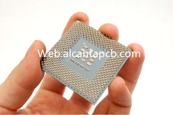
¿Qué son los sustratos del paquete FC-LGA??
Sustrato del paquete FC-LGA (Matriz de cuadrícula terrestre Flip Chip Sustratos de paquete) Es una tecnología de embalaje clave en la fabricación electrónica moderna.. Conecta el chip directamente a una matriz de rejilla de pines en el sustrato dándole la vuelta para una conexión eficiente de componentes electrónicos.. Esta tecnología de embalaje no sólo mejora significativamente el rendimiento eléctrico, pero también mejora en gran medida la confiabilidad y estabilidad del sistema.
En el sustrato de embalaje FC-LGA, la superficie activa del chip (la superficie del circuito en la oblea) mira hacia el sustrato, y las conexiones de circuitos de alta densidad se logran a través de un pequeño espacio entre pines y procesos de fabricación precisos.. Este diseño no sólo reduce efectivamente el tamaño del paquete, sino que también mejora la velocidad y la estabilidad de la transmisión de la señal. Es especialmente adecuado para aplicaciones en equipos informáticos y de comunicación de alto rendimiento que requieren una velocidad de procesamiento de datos y una eficiencia de consumo de energía extremadamente altas..
El proceso de fabricación de FC-LGA sustratos de embalaje implica pasos de proceso complejos, incluida la selección del material del sustrato y el pretratamiento, deposición de capa de cobre y galvanoplastia, patrones de fotolitografía, y soldadura final y pruebas.. Estos pasos no sólo requieren equipos y tecnología de fabricación de alta precisión, pero también requieren un control estricto de cada enlace para garantizar la calidad y estabilidad del producto empaquetado..
En equipos electrónicos modernos., Los sustratos de embalaje FC-LGA se utilizan ampliamente en varias computadoras de alto rendimiento, servidores, equipos de red y equipos de comunicación. Su rendimiento eléctrico superior y su confiabilidad lo convierten en una opción ideal para satisfacer necesidades complejas de procesamiento de datos y requisitos de operación estable a largo plazo.. A través de sustratos de embalaje FC-LGA, Los equipos electrónicos no solo pueden lograr una mayor integración y rendimiento., sino que también reduce eficazmente el consumo de energía y los costos de mantenimiento del sistema general, promoviendo así el desarrollo y aplicación de la tecnología electrónica moderna.
Guía de referencia de diseño de sustratos del paquete FC-LGA.
Sustratos del paquete FC-LGA (Sustratos del paquete Flip Chip Land Grid Array) Desempeñan un papel vital en el diseño electrónico moderno.. Sus características y ventajas de diseño únicas la convierten en una de las tecnologías preferidas en campos como las computadoras y servidores de alto rendimiento..
Las características clave del diseño del sustrato del paquete FC-LGA incluyen diseño de alta densidad y gestión térmica optimizada.. A través de un pequeño espacio entre pines y tecnología de apilamiento multicapa, el sustrato de embalaje FC-LGA logra conexiones de chip altamente integradas, compatible con circuitos integrados a gran escala y aplicaciones de alta frecuencia. Al mismo tiempo, El diseño optimizado de disipación de calor y la selección de materiales mejoran eficazmente el efecto de disipación de calor y cumplen con los requisitos del funcionamiento a largo plazo del equipo con carga alta..
El proceso de fabricación del sustrato de embalaje FC-LGA pasa por múltiples procesos de precisión, incluyendo la selección del material del sustrato, deposición de capa de cobre, patrones de fotolitografía, galvanoplastia, perforación, montaje y soldadura. Cada paso sigue estrictamente procesos de producción estandarizados y automatizados para garantizar la calidad y estabilidad del producto..
Los sustratos de empaquetado FC-LGA se utilizan ampliamente en computadoras de alto rendimiento, servidores, equipo de red, Equipos de comunicación y otros campos.. Su excelente rendimiento eléctrico y estabilidad pueden satisfacer necesidades complejas de comunicación y procesamiento de datos., proporcionando soporte clave para la infraestructura moderna de tecnología de la información.
El sustrato de embalaje FC-LGA tiene ventajas obvias sobre la tecnología de embalaje tradicional, incluyendo integración y rendimiento mejorados, utilización optimizada del espacio, y alta confiabilidad y estabilidad. Estas ventajas hacen que el sustrato de embalaje FC-LGA sea la primera opción para el diseño de muchos equipos electrónicos de alta gama., Promover el desarrollo y la innovación de la tecnología electrónica..
A través de esta guía, Los ingenieros de diseño y los profesionales de la tecnología electrónica pueden tener una comprensión profunda de los principios de diseño., Procesos de fabricación y escenarios de aplicación de sustratos de embalaje FC-LGA., y proporcionar referencia y orientación importantes para su aplicación en proyectos reales..
¿Qué material se utiliza en los sustratos del paquete FC-LGA??
La selección de materiales de los sustratos del paquete FC-LGA. (Sustratos del paquete Flip Chip Land Grid Array) es crucial y afecta directamente a su rendimiento eléctrico, efecto de disipación de calor y confiabilidad. Generalmente, Los principales materiales utilizados en los sustratos de embalaje FC-LGA incluyen resinas de alto rendimiento y conductores metálicos para satisfacer las necesidades de los modernos equipos informáticos y de comunicación de alto rendimiento..
Primero, El material base del sustrato suele ser una resina de alta calidad con excelente aislamiento eléctrico y resistencia mecánica.. Los materiales comunes incluyen FR4 (resina epoxi reforzada con fibra de vidrio) y materiales más avanzados como la poliimida (poliimida), que es particularmente adecuado para sustratos de embalaje FC-LGA flexibles y puede permanecer en su lugar bajo flexión o deflexión local. Estabilidad y conexiones eléctricas..
En segundo lugar, para lograr un diseño de componentes electrónicos de alta densidad y un diseño de circuito complejo, Los sustratos de embalaje FC-LGA suelen utilizar tecnología de apilamiento multicapa. Esta tecnología no sólo puede acomodar más componentes de circuito en un espacio limitado, sino que también reduce eficazmente los retrasos de la señal y la diafonía, mejorar la eficiencia y confiabilidad del sistema general.
En términos de la capa conductora., La parte clave del sustrato de embalaje FC-LGA es la formación de la rejilla de pines a través de la capa de cobre.. Se eligió el cobre como principal material conductor debido a su excelente conductividad y buena procesabilidad., y su capacidad para transportar y transmitir señales de alta frecuencia y grandes corrientes al mismo tiempo que proporciona conexiones eléctricas confiables.
En breve, La selección de materiales y el diseño del proceso del sustrato de embalaje FC-LGA son una parte importante de los equipos electrónicos modernos., que determina directamente el efecto de su aplicación y el rendimiento de confiabilidad en campos como las computadoras de alto rendimiento, servidores, y equipos de comunicación. En el futuro, con el avance de la tecnología y la continua evolución de las necesidades, Los sustratos de embalaje FC-LGA seguirán desempeñando un papel clave en la industria electrónica, Proporciona soporte estable y duradero para diversos dispositivos electrónicos de alto rendimiento y alta densidad..
¿De qué tamaño son los sustratos del paquete FC-LGA??
Sustratos del paquete FC-LGA (Sustratos del paquete Flip Chip Land Grid Array) Son ampliamente utilizados en el campo de la electrónica moderna por su alto rendimiento y confiabilidad.. Sus tamaños varían según los requisitos de la aplicación y el diseño del equipo.. En general, El tamaño del sustrato de embalaje FC-LGA depende del tipo de embalaje de chip utilizado y de los requisitos específicos del equipo..
En ordenadores de alto rendimiento, servidores y equipos de comunicación, Los sustratos de embalaje FC-LGA suelen diseñarse en formas cuadradas o rectangulares con dimensiones variables.. El tamaño de estos sustratos normalmente varía desde unos pocos milímetros hasta decenas de milímetros para adaptarse a diferentes escenarios de aplicación y limitaciones de espacio del dispositivo.. La selección del tamaño tiene en cuenta el nivel de integración de los componentes electrónicos., requisitos de disipación de calor, y el diseño general del dispositivo.
Por ejemplo, para circuitos integrados de alta densidad y dispositivos que requieren una gran cantidad de conexiones de E/S, El sustrato del paquete FC-LGA puede ser más grande para acomodar más pines y puntos de conexión.. De lo contrario, para dispositivos móviles y sistemas integrados, Los sustratos de embalaje FC-LGA más pequeños son más adecuados para lograr un diseño compacto y eficiencia espacial de los dispositivos..
Además, El tamaño del sustrato de embalaje FC-LGA también se ve afectado por la tecnología y los procesos de fabricación.. Los procesos de fabricación modernos permiten una mayor precisión y dimensiones más pequeñas, permitiendo que los sustratos alcancen tamaños físicos más pequeños sin sacrificar el rendimiento y la confiabilidad.
En general, El tamaño de los sustratos de embalaje FC-LGA continúa evolucionando con los avances tecnológicos y los cambios en la demanda del mercado.. Optimizando los procesos de diseño y fabricación., Estos sustratos pueden desempeñar un papel importante en varios dispositivos electrónicos., proporcionando un rendimiento eléctrico estable y capacidades eficientes de transmisión de datos, apoyando así el desarrollo de modernas tecnologías informáticas y de comunicación de alto rendimiento.
El proceso de fabricación de sustratos encapsulados FC-LGA.
Sustratos del paquete FC-LGA (Sustratos del paquete Flip Chip Land Grid Array) Juegan un papel importante en los dispositivos electrónicos modernos.. Sus tamaños varían según la aplicación y cubren ampliamente una variedad de requisitos de tamaño.. Estos sustratos de embalaje suelen diseñarse en formas cuadradas o rectangulares con una amplia gama de tamaños, desde pequeños hasta grandes, para satisfacer las necesidades de diseño de diferentes dispositivos y productos electrónicos..
En ordenadores de alto rendimiento, servidores y equipos de red, Los sustratos de empaque FC-LGA suelen ser más grandes y pueden alcanzar decenas de centímetros de largo para acomodar circuitos complejos y conexiones multicapa.. Estos sustratos de gran tamaño no solo admiten más componentes electrónicos y diseños de circuitos complejos, sino que también reduce eficazmente la acumulación de calor dentro de los dispositivos electrónicos y mejora el rendimiento general y la confiabilidad..
Relativamente hablando, Sustratos de embalaje FC-LGA utilizados en productos electrónicos de consumo como teléfonos inteligentes, tabletas, y los dispositivos electrónicos portátiles suelen ser más pequeños para adaptarse a los requisitos de diseño compacto del dispositivo.. Estos sustratos de pequeño tamaño no sólo requieren un diseño de chip altamente integrado, pero también requiere que se consideren el espacio de la batería y el peso ligero del dispositivo.. Por lo tanto, el tamaño es generalmente pequeño, generalmente entre unos pocos centímetros y más de diez centímetros.
Independientemente del tamaño, La clave para el diseño del sustrato del paquete FC-LGA es tener en cuenta la optimización del diseño del circuito y el uso eficaz del espacio físico.. A través de tecnología de proceso avanzada y selección de materiales., Estos sustratos son capaces de admitir conexiones de chips de alta densidad y funciones electrónicas complejas al tiempo que garantizan la estabilidad y confiabilidad del rendimiento eléctrico..
En general, El tamaño del sustrato de embalaje FC-LGA depende de las necesidades específicas de la aplicación y de los requisitos de diseño del dispositivo.. Desde pequeños dispositivos portátiles hasta grandes sistemas de servidores, Se puede encontrar un tamaño de sustrato de embalaje adecuado para admitir las diversas funciones y funciones de los productos electrónicos modernos.. Requisitos de desempeño.
El área de aplicación de los sustratos encapsulados FC-LGA.
Sustratos del paquete FC-LGA (Sustratos del paquete Flip Chip Land Grid Array) Son ampliamente utilizados en equipos electrónicos modernos., y sus características de diseño superiores los convierten en una opción ideal para equipos informáticos y de comunicación de alto rendimiento.. Las siguientes son las principales áreas de aplicación de los sustratos de embalaje FC-LGA.:
Los sustratos de embalaje FC-LGA se utilizan ampliamente en computadoras y servidores de alto rendimiento debido a sus conexiones de alta densidad y gestión térmica optimizada.. Estos campos tienen demandas crecientes de procesamiento de datos a gran escala y tareas informáticas complejas.. Los sustratos de embalaje FC-LGA pueden admitir una transmisión de datos rápida y un funcionamiento estable, mejorar el rendimiento general y la eficiencia del sistema.
En equipos de red y equipos de comunicación., Los sustratos de embalaje FC-LGA se utilizan ampliamente para satisfacer las necesidades de transmisión de datos de alta velocidad y comunicación estable.. Ya sean enrutadores, interruptores o equipos de comunicación de fibra óptica, Estos escenarios de aplicación requieren tecnología de embalaje que pueda proporcionar conexiones eléctricas confiables y resistencia ambiental a altas temperaturas.. Los sustratos de embalaje FC-LGA pueden cumplir eficazmente estos requisitos.
En sistemas de control y automatización industrial, La alta confiabilidad y estabilidad de los sustratos de empaque FC-LGA los convierten en la primera opción para componentes clave como controladores., sensores y actuadores. Estas aplicaciones requieren que los equipos funcionen durante mucho tiempo y resistan duras condiciones ambientales industriales.. Los sustratos de embalaje FC-LGA pueden proporcionar durabilidad y confiabilidad duraderas mientras mantienen el rendimiento..
En equipos médicos e instrumentos científicos., Los sustratos de embalaje FC-LGA se utilizan en diversas mediciones complejas y de alta precisión., equipos de seguimiento y tratamiento. Estas aplicaciones tienen requisitos extremadamente altos en cuanto a la precisión, Estabilidad y seguridad de los sistemas electrónicos.. El sustrato de embalaje FC-LGA puede garantizar un funcionamiento confiable del equipo y una recopilación de datos precisa a través de su avanzado diseño y tecnología de fabricación..
En breve, El sustrato de embalaje FC-LGA ha demostrado su posición clave y su papel insustituible en la tecnología electrónica moderna con su amplia aplicación en informática de alto rendimiento., comunicaciones, controles industriales, y la investigación médica. Con el avance de la tecnología y el crecimiento de la demanda del mercado., Se espera que los sustratos de embalaje FC-LGA sigan desempeñando un papel importante en el futuro., promover la mejora continua del rendimiento y funciones de diversos dispositivos electrónicos.
¿Cuáles son las ventajas de los sustratos encapsulados FC-LGA??
Como componente clave en equipos electrónicos modernos., Sustratos del paquete FC-LGA (Sustratos del paquete Flip Chip Land Grid Array) tener múltiples ventajas, haciéndolos ampliamente utilizados en equipos informáticos y de comunicación de alto rendimiento..
Primero, El sustrato de embalaje FC-LGA permite conexiones de alta densidad volteando el chip directamente y conectándolo a la matriz de rejilla de pines del sustrato.. Este diseño puede acomodar más pines de chip en un espacio limitado y admitir una mayor integración y un diseño de circuito más complejo.. En circuitos integrados a gran escala y aplicaciones de alta frecuencia., Los sustratos de embalaje FC-LGA demuestran ventajas de rendimiento superiores y garantizan la estabilidad y confiabilidad de la transmisión de datos..
En segundo lugar, El sustrato de embalaje FC-LGA tiene un rendimiento excepcional en la gestión térmica.. Mediante un diseño optimizado de disipación de calor y selección de materiales, Resuelve eficazmente el problema de calor generado en equipos de alto rendimiento.. Esto no sólo ayuda a prolongar la vida útil del dispositivo, sino que también garantiza el rendimiento estable del dispositivo durante el funcionamiento a largo plazo, Lo cual es especialmente importante en escenarios que requieren un funcionamiento estable durante mucho tiempo., como servidores y equipos de red.
Además, El proceso de fabricación de los sustratos de embalaje FC-LGA se controla con precisión para garantizar la consistencia y confiabilidad del producto.. Desde la selección del material del sustrato hasta la deposición de la capa de cobre., procesamiento de fotolitografía, galvanoplastia, perforación, para montaje y soldadura, Cada paso se somete a estrictos controles de calidad y pruebas para garantizar que el producto final cumpla con altos estándares de requisitos de rendimiento eléctrico y mecánico..
Finalmente, Los sustratos de embalaje FC-LGA tienen una amplia gama de aplicaciones, cubriendo muchos campos como las computadoras de alto rendimiento, servidores, equipo de red, y equipos de comunicación. Su excelente rendimiento eléctrico y estabilidad lo convierten en una opción ideal para procesamiento de datos complejos y necesidades de comunicación de alta velocidad., Proporcionar un apoyo importante para la mejora del rendimiento y la optimización del diseño de diversos dispositivos electrónicos modernos..
En resumen, Sustrato de embalaje FC-LGA, con sus múltiples ventajas como conexiones de alta densidad, gestión térmica optimizada, Procesos de fabricación de precisión y amplia gama de aplicaciones., no solo promueve el progreso del rendimiento de los equipos electrónicos, sino que también proporciona innovación tecnológica y competencia en el mercado.. una base sólida.
Preguntas frecuentes
¿Qué es el sustrato de embalaje FC-LGA??
Sustrato del paquete FC-LGA (Sustratos del paquete Flip Chip Land Grid Array) es una tecnología avanzada de conexión de componentes electrónicos que logra conexiones eléctricas de alta densidad y alto rendimiento volteando directamente el chip y conectándolo a la matriz de rejilla de pines en el sustrato.. Esta tecnología de embalaje es especialmente adecuada para aplicaciones que requieren transmisión de datos de alta velocidad y gestión térmica optimizada..
¿Cuáles son las características de diseño del sustrato de embalaje FC-LGA??
Las características de diseño del sustrato del paquete FC-LGA incluyen un diseño de pines de alta densidad, soporte para pines de paso fino y tecnología de apilamiento multicapa para lograr una mayor integración y velocidades de transmisión de señal más rápidas. Además, El diseño optimizado de gestión térmica reduce eficazmente las temperaturas de los componentes y mejora la confiabilidad de la operación a largo plazo..
¿Cuál es el proceso de fabricación del sustrato de embalaje FC-LGA??
El proceso de fabricación de sustratos de embalaje FC-LGA incluye múltiples procesos, como la selección del material del sustrato., deposición de capa de cobre, patrones de fotolitografía, galvanoplastia, perforación, montaje y soldadura. Cada paso requiere un control preciso del proceso para garantizar la calidad y estabilidad del producto final..
¿En qué campos se utilizan principalmente los sustratos de embalaje FC-LGA??
Los sustratos de empaquetado FC-LGA se utilizan ampliamente en computadoras de alto rendimiento, servidores, equipo de red, Equipos de comunicación y otros campos.. Su transmisión de señal de alta velocidad y sus capacidades de gestión térmica optimizadas lo hacen especialmente adecuado para entornos que requieren procesamiento de big data y tiempos de operación prolongados..