CO.,LTD")
Flip-Chip (ABF) Substrathersteller.Flip Chip (ABF) Substrathersteller sind auf die Herstellung fortschrittlicher Aufbaufolien spezialisiert (ABF) Substrate, unerlässlich für Hochleistungs-Halbleiterverpackungen. Diese Substrate ermöglichen Verbindungen mit höherer Dichte und ein verbessertes Wärmemanagement, entscheidend für Anwendungen in der Informatik, Telekommunikation, und Automobilindustrie. Führende Hersteller nutzen modernste Technologie und strenge Qualitätskontrollen, um zuverlässig zu liefern, hochpräzise ABF-Substrate, Gewährleistung optimaler Leistung und Effizienz in modernen elektronischen Geräten.
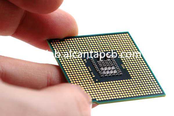
Flip-Chip (ABF) Die Untergründe sind fortgeschritten Verpackung Materialien zur Montage und Verbindung integrierter Schaltkreise (ICs) mit Flip-Chip-Technologie. Diese Substrate sind für Hochleistungshalbleiteranwendungen von entscheidender Bedeutung, Bereitstellung einer verbesserten elektrischen Leistung, Wärmemanagement, und Miniaturisierungsfähigkeiten. Dieser Artikel befasst sich mit den Merkmalen, Konstruktionsüberlegungen, Materialien, Herstellungsprozesse, Anwendungen, und Vorteile von Flip-Chip (ABF) Substrate.
Was sind Flip-Chip? (ABF) Substrate?
Flip-Chip (ABF) Substrate sind spezielle Verpackungssubstrate, die die Flip-Chip-Technologie nutzen, Dabei wird der IC mit der Vorderseite nach unten auf das Substrat montiert, Ermöglicht direkte elektrische Verbindungen über Löthöcker. ABF (Ajinomoto Aufbaufilm) ist ein dielektrisches Hochleistungsmaterial, das in diesen Substraten verwendet wird, um feine Linien- und Raumeigenschaften zu erreichen, unerlässlich für fortschrittliche Halbleitergeräte. Diese Substrate werden häufig in hoher Dichte verwendet, Hochgeschwindigkeitsanwendungen wie Prozessoren, Speichergeräte, und fortschrittliche Kommunikationssysteme.
Designüberlegungen für Flip-Chip (ABF) Substrate
Flip-Chip entwerfen (ABF) Untergründe erfordern mehrere wichtige Überlegungen:
Auswahl der richtigen Materialien mit geeigneten dielektrischen Eigenschaften, Wärmeleitfähigkeit, und die mechanische Festigkeit ist entscheidend für eine optimale Leistung.
Um eine Überhitzung zu verhindern und einen zuverlässigen Betrieb zu gewährleisten, ist ein effizientes Wärmemanagement unerlässlich. Dazu gehört auch die Einbindung thermischer Vias, Wärmespreizner, und andere Kühlmechanismen.
Die Aufrechterhaltung der Signalintegrität bei hohen Frequenzen erfordert eine sorgfältige Kontrolle der Spurenimpedanz, Minimierung des Übersprechens, und Implementierung wirksamer Erdungs- und Abschirmtechniken.
Der Untergrund muss über ausreichende mechanische Festigkeit und Stabilität verfügen, um Herstellungsprozessen und Betriebsbedingungen standzuhalten, einschließlich thermischer Zyklen und mechanischer Beanspruchung.
Die Oberflächenbeschaffenheit muss glatt und fehlerfrei sein, um eine ordnungsgemäße Haftung und Ausrichtung der Komponenten zu gewährleisten und Signalverluste und Reflexionen zu minimieren.
Materialien, die im Flip Chip verwendet werden (ABF) Substrate
Bei der Herstellung von Flip-Chips werden üblicherweise mehrere Materialien verwendet (ABF) Substrate:
ABF ist ein dielektrisches Hochleistungsmaterial, das hervorragende elektrische Eigenschaften bietet, Feinlinienfähigkeiten, und mechanische Festigkeit.
Für die Leiterbahnen und Vias wird hochwertige Kupferfolie verwendet, bietet hervorragende elektrische Leitfähigkeit und Zuverlässigkeit.
Als Klebematerialien werden Hochleistungs-Epoxidharze eingesetzt, um die Schichten des Untergrundes miteinander zu verbinden, Bereitstellung mechanischer Stärke und Stabilität.
Diese werden auf die Kontaktpads angewendet, um die Lötlichkeit zu verbessern und vor Oxidation zu schützen.
In einigen Fällen, Keramik wie Aluminiumoxid (AL2O3) oder Aluminiumnitrid (AlN) können aufgrund ihrer hervorragenden Wärmeleitfähigkeit und mechanischen Eigenschaften verwendet werden.
Herstellungsprozess des Flip-Chips (ABF) Substrate
Der Herstellungsprozess von Flip Chip (ABF) Die Herstellung von Substraten erfordert mehrere präzise Schritte:
Die Rohstoffe, einschließlich ABF, Kupferfolie, und Epoxidharze, werden aufbereitet und zu Platten oder Rollen verarbeitet.
Mehrere Schichten des Substratmaterials werden zusammen laminiert, um eine Aufbaustruktur zu bilden. Bei diesem Vorgang werden Wärme und Druck angewendet, um die Schichten zu verbinden.
Schaltungsmuster werden unter Verwendung photolithographischer Prozesse erzeugt. Ein photosensitiver Film (Fotolack) wird auf das Substrat angewendet, Ultraviolett ausgesetzt (UV) Licht durch eine Maske, und entwickelt, um die gewünschten Schaltungsmuster aufzudecken. Das Substrat wird dann geätzt, um unerwünschtes Material zu entfernen.
VIAS werden in das Substrat gebohrt, um vertikale elektrische Verbindungen zwischen verschiedenen Schichten herzustellen. Diese Löcher werden dann mit Kupfer plattiert, um leitende Pfade herzustellen.
Eine glatte, Auf die Kontaktpads wird eine fehlerfreie Oberflächenveredelung aufgetragen, um eine ordnungsgemäße Haftung und Ausrichtung der Komponenten sicherzustellen, sowie zur Minimierung von Signalverlust und Reflexion.
Die fertigen Substrate werden strengen Tests und Inspektionen unterzogen, um sicherzustellen, dass sie die erforderlichen Spezifikationen für die elektrische Leistung erfüllen, Signalintegrität, und Zuverlässigkeit.
Anwendungen von Flip Chip (ABF) Substrate
Flip-Chip (ABF) Substrate werden in einer Vielzahl von Hochleistungsanwendungen eingesetzt:
Diese Substrate werden in Hochleistungsprozessoren und Mikrocontrollern eingesetzt, Bereitstellung der notwendigen elektrischen und thermischen Eigenschaften für einen zuverlässigen Betrieb.
Flip-Chip (ABF) Substrate werden in Speichergeräten verwendet, einschließlich DRAM und Flash-Speicher, wo hochdichte Verbindungen und Signalintegrität von entscheidender Bedeutung sind.
Diese Substrate unterstützen fortschrittliche Kommunikationssysteme, einschließlich 5G -Basisstationen und Netzwerkinfrastruktur, wo Hochgeschwindigkeitsbetrieb und Signalintegrität unerlässlich sind.
Flip-Chip (ABF) Substrate werden in der Unterhaltungselektronik eingesetzt, wie Smartphones, Tabletten, und tragbare Geräte, wo Miniaturisierung und Leistung entscheidend sind.
Die Substrate werden in der Automobilelektronik eingesetzt, einschließlich fortschrittlicher Fahrerassistenzsysteme (Adas) und Infotainmentsysteme, erfordern robuste Leistung und Zuverlässigkeit.
Vorteile von Flip Chip (ABF) Substrate
Flip-Chip (ABF) Substrate bieten mehrere Vorteile:
Die Verwendung von ABF ermöglicht feine Linien- und Raummerkmale, Dies ermöglicht hochdichte Verbindungen, die für fortschrittliche Halbleiterbauelemente erforderlich sind.
Diese Substrate bieten eine hervorragende elektrische Leistung, einschließlich geringem Signalverlust und hoher Signalintegrität, entscheidend für Hochgeschwindigkeitsanwendungen.
Materialien mit hoher Wärmeleitfähigkeit sorgen für eine effiziente Wärmeableitung, Vermeidung von Überhitzung und Gewährleistung eines zuverlässigen Betriebs.
Die Substrate bieten eine robuste mechanische Unterstützung, Gewährleistung der Zuverlässigkeit und Haltbarkeit der verpackten Komponenten unter verschiedenen Umgebungsbedingungen.
Die Fähigkeit, feine Strukturen und hochdichte Verbindungen zu schaffen, unterstützt die Miniaturisierung von Halbleitergehäusen, Dadurch sind sie für kompakte elektronische Geräte geeignet.
FAQ
Was sind die Hauptvorteile der Verwendung von Flip Chip? (ABF) Substrate?
Zu den Hauptvorteilen gehören Verbindungen mit hoher Dichte, Überlegene elektrische Leistung, effizientes Thermomanagement, mechanische Stabilität, und Unterstützung der Miniaturisierung. Diese Substrate bilden die Grundlage für die Herstellung leistungsstarker Halbleiterbauelemente.
Welche Materialien werden üblicherweise in Flip Chip verwendet? (ABF) Substrate?
Zu den gängigen Materialien gehört ABF (Ajinomoto Aufbaufilm), Kupferfolie, Hochleistungs-Epoxidharze, Nickel/Gold-Oberflächen, Und, in manchen Fällen, Hochleistungskeramiken wie Aluminiumoxid oder Aluminiumnitrid.
Wie funktioniert das Design eines Flip Chips? (ABF) Das Substrat gewährleistet die Signalintegrität?
Das Design gewährleistet die Signalintegrität durch niedrige Werte für Dielektrizitätskonstante und Verlustfaktor, Kontrolle der Spurenimpedanz, Minimierung des Übersprechens, und Implementierung wirksamer Erdungs- und Abschirmtechniken. Simulationstools werden verwendet, um diese Aspekte für die Hochfrequenzleistung zu optimieren.
Was sind die häufigsten Anwendungen von Flip Chip? (ABF) Substrate?
Zu den gängigen Anwendungen gehören Prozessoren und Mikrocontroller, Speichergeräte, fortgeschrittene Kommunikationssysteme, Unterhaltungselektronik, und Automobilelektronik. Diese Substrate werden in Systemen verwendet, die hochdichte Verbindungen erfordern, Überlegene elektrische Leistung, und effizientes Wärmemanagement.