CO.,LTD")
Hersteller von RF-Paketsubstraten.An RF Paketsubstrate Der Hersteller ist auf die Herstellung von Hochleistungssubstraten für HF-Anwendungen spezialisiert, Dies ermöglicht eine effiziente Signalübertragung und ein hervorragendes Wärmemanagement. Mit fortschrittlichen Fertigungstechniken, Sie bieten maßgeschneiderte Lösungen, um den hohen Anforderungen der Telekommunikation gerecht zu werden, Luft- und Raumfahrt, und Verteidigungsindustrie. Ihr Fachwissen gewährleistet Zuverlässigkeit und verbesserte Leistung in kritischen HF-Systemen.
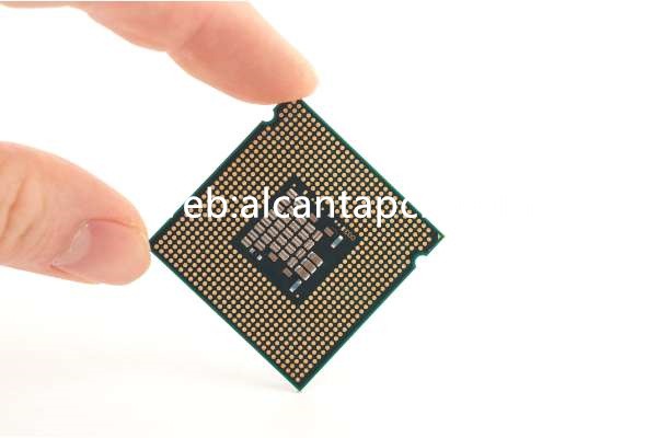
Rf (Funkfrequenz) Paket Substrate sind wesentliche Komponenten bei der Herstellung elektronischer Geräte, die mit Funkfrequenzen arbeiten, einschließlich drahtloser Kommunikationssysteme, Radar, und Satellitenkommunikation. Diese Substrate sind für eine hervorragende Signalintegrität ausgelegt, Wärmemanagement, und mechanische Stabilität, Damit sind sie ideal für Hochfrequenzanwendungen. In diesem Artikel werden die Funktionen erläutert, Konstruktionsüberlegungen, Materialien, Herstellungsprozesse, Anwendungen, und Vorteile von RF-Gehäusesubstraten.
Was sind RF-Paketsubstrate??
HF-Gehäusesubstrate sind spezielle Materialien, die bei der Verpackung elektronischer HF-Komponenten verwendet werden. Sie dienen als Grundlage für die Montage und Verbindung verschiedener elektronischer Geräte, einschließlich integrierter Schaltkreise (ICs), Widerstände, Kondensatoren, und Induktoren. Diese Substrate sind so konstruiert, dass Signalverluste und -verzerrungen minimiert werden, sorgen für ein effizientes Thermomanagement, und bieten mechanische Unterstützung. Sie sind entscheidend für die Aufrechterhaltung der Leistung und Zuverlässigkeit von HF-Systemen.
Designüberlegungen für HF-Gehäusesubstrate
Das Entwerfen von HF-Gehäusesubstraten erfordert mehrere wichtige Überlegungen:
Auswahl der richtigen Materialien mit geeigneten dielektrischen Eigenschaften, Wärmeleitfähigkeit, und die mechanische Festigkeit ist entscheidend für eine optimale Leistung.
Um eine Überhitzung zu verhindern und einen zuverlässigen Betrieb zu gewährleisten, ist ein effizientes Wärmemanagement unerlässlich. Dazu gehört auch die Einbindung thermischer Vias, Wärmespreizner, und andere Kühlmechanismen.
Die Aufrechterhaltung der Signalintegrität bei hohen Frequenzen erfordert eine sorgfältige Kontrolle der Spurenimpedanz, Minimierung des Übersprechens, und Implementierung wirksamer Erdungs- und Abschirmtechniken.
Der Untergrund muss über ausreichende mechanische Festigkeit und Stabilität verfügen, um Herstellungsprozessen und Betriebsbedingungen standzuhalten, einschließlich thermischer Zyklen und mechanischer Beanspruchung.
Die Oberflächenbeschaffenheit muss glatt und fehlerfrei sein, um eine ordnungsgemäße Haftung und Ausrichtung der Komponenten zu gewährleisten und Signalverluste und Reflexionen zu minimieren.
Materialien, die in HF-Gehäusesubstraten verwendet werden
Bei der Herstellung von HF-Gehäusesubstraten werden üblicherweise mehrere Materialien verwendet:
Materialien wie Aluminiumoxid (AL2O3), Aluminiumnitrid (AlN), und Berylliumoxid (BeO) bieten hervorragende dielektrische Eigenschaften und eine hohe Wärmeleitfähigkeit.
Hochfrequenzlaminate, wie PTFE (Polytetrafluorethylen) und keramisch gefüllte PTFE-Verbundwerkstoffe, sorgen für niedrige Dielektrizitätskonstanten und Verlustfaktorwerte, Gewährleistung minimaler Signalverluste.
Aufgrund ihrer hervorragenden elektrischen Leitfähigkeit und Zuverlässigkeit werden Kupfer und andere Metalllegierungen für Leiterbahnen und Durchkontaktierungen verwendet.
Als Klebematerialien werden Hochleistungs-Epoxidharze eingesetzt, um die Schichten des Untergrundes miteinander zu verbinden, Bereitstellung mechanischer Stärke und Stabilität.
Diese werden auf die Kontaktpads angewendet, um die Lötlichkeit zu verbessern und vor Oxidation zu schützen.
Herstellungsprozess von HF-Gehäusesubstraten
Der Herstellungsprozess von HF-Gehäusesubstraten umfasst mehrere präzise Schritte:
Die Rohstoffe, einschließlich Hochleistungskeramik, organische Laminate, und Metalllegierungen, werden zu Blättern oder Filmen vorbereitet und verarbeitet.
Mehrere Schichten des Substratmaterials werden zusammen laminiert, um eine Aufbaustruktur zu bilden. Bei diesem Vorgang werden Wärme und Druck angewendet, um die Schichten zu verbinden.
Schaltungsmuster werden unter Verwendung photolithographischer Prozesse erzeugt. Ein photosensitiver Film (Fotolack) wird auf das Substrat angewendet, Ultraviolett ausgesetzt (UV) Licht durch eine Maske, und entwickelt, um die gewünschten Schaltungsmuster aufzudecken. Das Substrat wird dann geätzt, um unerwünschtes Material zu entfernen.
VIAS werden in das Substrat gebohrt, um vertikale elektrische Verbindungen zwischen verschiedenen Schichten herzustellen. Diese Löcher werden dann mit Kupfer plattiert, um leitende Pfade herzustellen.
Eine glatte, Auf die Kontaktpads wird eine fehlerfreie Oberflächenveredelung aufgetragen, um eine ordnungsgemäße Haftung und Ausrichtung der Komponenten sicherzustellen, sowie zur Minimierung von Signalverlust und Reflexion.
Die fertigen Substrate werden strengen Tests und Inspektionen unterzogen, um sicherzustellen, dass sie die erforderlichen Spezifikationen für die elektrische Leistung erfüllen, Signalintegrität, und Zuverlässigkeit.
Anwendungen von HF-Gehäusesubstraten
HF-Gehäusesubstrate werden in einer Vielzahl von Hochfrequenzanwendungen eingesetzt:
Diese Substrate unterstützen die Verpackung von HF-Komponenten in Mobiltelefonen, Basisstationen, WLAN-Router, und andere drahtlose Kommunikationsgeräte.
HF-Gehäusesubstrate werden in Radarsystemen im Automobilbereich eingesetzt, Luftfahrt, und Verteidigungsanwendungen, wo Hochfrequenzbetrieb und Zuverlässigkeit entscheidend sind.
Diese Substrate werden in Satellitenkommunikationssystemen verwendet, einschließlich Satellitentransponder und Bodenstationsausrüstung, Gewährleistung einer hohen Signalintegrität und Leistung.
HF-Gehäusesubstrate werden in medizinischen Geräten und Geräten verwendet, wie MRT-Geräte und drahtlose Patientenüberwachungssysteme, wo ein zuverlässiger Hochfrequenzbetrieb unerlässlich ist.
Die Substrate werden in Luft- und Raumfahrt- und Verteidigungsanwendungen eingesetzt, einschließlich Kommunikationssystemen, elektronische Kriegsführung, und Leitsysteme, wo robuste Leistung und Zuverlässigkeit erforderlich sind.
Vorteile von RF-Paketsubstraten
RF-Gehäusesubstrate bieten mehrere Vorteile:
Die niedrige Dielektrizitätskonstante und der Verlustfaktor sorgen für minimale Signalverluste und -verzerrungen, Aufrechterhaltung einer hohen Signaltreue und Leistung.
Materialien mit hoher Wärmeleitfähigkeit sorgen für eine effiziente Wärmeableitung, Vermeidung von Überhitzung und Gewährleistung eines zuverlässigen Betriebs.
Die Substrate bieten eine robuste mechanische Unterstützung, Gewährleistung der Zuverlässigkeit und Haltbarkeit der verpackten Komponenten unter verschiedenen Umgebungsbedingungen.
HF-Gehäusesubstrate sind mit einer Vielzahl von HF-Komponenten kompatibel und können verschiedene Montage- und Verbindungstechniken unterstützen.
Diese Substrate können an spezifische Designanforderungen angepasst werden, einschließlich der Einarbeitung spezifischer Materialien, Schichtkonfigurationen, und Oberflächenveredelungen.
FAQ
Was sind die Hauptvorteile der Verwendung von RF-Paketsubstraten??
Zu den Hauptvorteilen zählt die hohe Signalintegrität, effizientes Thermomanagement, mechanische Stabilität, Kompatibilität mit HF-Komponenten, und Anpassbarkeit. Diese Substrate bilden die Grundlage für die Herstellung leistungsstarker elektronischer HF-Geräte mit zuverlässiger Signalintegrität und effizientem Wärmemanagement.
Welche Materialien werden üblicherweise in HF-Gehäusesubstraten verwendet??
Zu den gängigen Materialien gehört Hochleistungskeramik (wie Aluminiumoxid, Aluminiumnitrid, und Berylliumoxid), organische Laminate (wie PTFE und keramisch gefüllte PTFE-Verbundwerkstoffe), Metalllegierungen (wie Kupfer), Epoxidharze, und Nickel/Gold -Oberflächen. Diese Materialien bieten hervorragende dielektrische Eigenschaften, Wärmeleitfähigkeit, und mechanische Festigkeit.
Wie stellt das Design eines RF-Gehäusesubstrats die Signalintegrität sicher??
Das Design gewährleistet die Signalintegrität durch niedrige Werte für Dielektrizitätskonstante und Verlustfaktor, Kontrolle der Spurenimpedanz, Minimierung des Übersprechens, und Implementierung wirksamer Erdungs- und Abschirmtechniken. Simulationstools werden verwendet, um diese Aspekte für die Hochfrequenzleistung zu optimieren.
Was sind die häufigsten Anwendungen von RF-Gehäusesubstraten??
Zu den üblichen Anwendungen gehören drahtlose Kommunikationssysteme, Radarsysteme, Satellitenkommunikation, Medizinprodukte, und Luft- und Raumfahrt und Verteidigung. Diese Substrate werden in Systemen verwendet, die eine hohe Signalintegrität erfordern, effizientes Thermomanagement, und robuste Leistung und Zuverlässigkeit.