CO., LTD")
Fabricante de sustrato Flip Chip BGA. Como líder Voltear chip Fabricante de sustrato BGA, Nos especializamos en producir sustratos de alta calidad diseñados para un rendimiento óptimo en la electrónica moderna.. Nuestro proceso de fabricación de última generación garantiza una gestión térmica superior., interconexiones de alta densidad, e integridad de la señal mejorada. Con la confianza de empresas tecnológicas de primer nivel, Ofrecemos soluciones confiables e innovadoras que satisfacen las estrictas demandas de la industria de semiconductores.. Con un compromiso con la excelencia., Avanzamos continuamente en nuestras tecnologías para respaldar la próxima generación de dispositivos electrónicos..
¿Qué es el sustrato BGA Flip Chip??
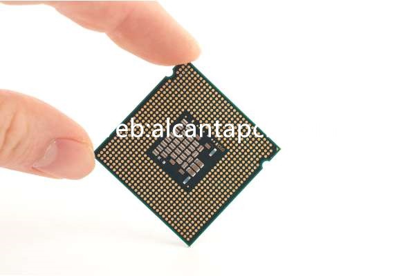
Matriz de cuadrícula de bolas con chip volteado (BGA) Los sustratos son componentes especializados que se utilizan para montar semiconductores de chip invertido en placas de circuito impreso. (PCB). A diferencia de la unión de cables tradicional, La tecnología de chip invertido implica unir directamente el lado activo del chip semiconductor al sustrato mediante una serie de protuberancias de soldadura.. Este método proporciona una ruta eléctrica más directa., reduciendo la inductancia de la señal y mejorando el rendimiento.
Los sustratos BGA con chip invertido son fundamentales en aplicaciones de alto rendimiento debido a su capacidad para manejar frecuencias más altas y una mayor disipación de calor.. Se utilizan en diversos dispositivos electrónicos., incluyendo procesadores, tarjetas graficas, y dispositivos de comunicación de alta velocidad.
Los tipos de sustratos BGA Flip Chip
Existen varios tipos de sustratos BGA con chip invertido, cada uno diseñado para satisfacer necesidades de aplicaciones específicas:
Sustratos Orgánicos: Fabricado con materiales orgánicos laminados como BT. (Bismaleimida triazina) resina o FR-4, Estos sustratos son rentables y ofrecen buenas propiedades mecánicas., haciéndolos adecuados para una amplia gama de aplicaciones.
Sustratos Cerámicos: Compuesto por materiales como alúmina o nitruro de aluminio., Los sustratos cerámicos proporcionan una excelente conductividad térmica y resistencia mecánica., ideal para aplicaciones de alta potencia y alta frecuencia.
Sustratos con núcleo metálico: Estos sustratos incorporan un núcleo metálico. (generalmente aluminio o cobre) para mejorar la disipación de calor. Se utilizan en aplicaciones de alta potencia donde la gestión térmica eficiente es crucial..
Sustratos rígidos-flexibles: Combinando capas rígidas y flexibles, Estos sustratos ofrecen versatilidad de diseño y se utilizan en dispositivos compactos donde las limitaciones de espacio requieren doblar y doblar la PCB..
Las ventajas de los sustratos BGA Flip Chip
Los sustratos BGA con chip invertido ofrecen varias ventajas, haciéndolos adecuados para aplicaciones electrónicas avanzadas:
La unión directa del chip al sustrato reduce la inductancia y la resistencia., Lo que lleva a un mejor rendimiento eléctrico y una mayor integridad de la señal..
Las protuberancias de soldadura proporcionan una ruta térmica directa desde el chip al sustrato., mejorando la disipación de calor y permitiendo mayores densidades de potencia.
Los sustratos BGA con chip invertido permiten diseños más compactos al eliminar la necesidad de uniones de cables y reducir el espacio total del paquete..
El uso de una serie de protuberancias de soldadura permite una mayor cantidad de conexiones de entrada/salida, compatible con dispositivos más complejos y potentes.
El método de fijación directa mejora la estabilidad mecánica del paquete., Reducir el riesgo de daños durante el montaje y el funcionamiento..
Cómo diseñar un sustrato BGA Flip Chip?
El diseño de un sustrato BGA con chip invertido implica varios pasos críticos para garantizar un rendimiento y una confiabilidad óptimos.:
Elija el material de sustrato adecuado según las condiciones térmicas de la aplicación., eléctrico, y requisitos mecánicos.
Diseñe el diseño de los puntos de soldadura para optimizar el rendimiento eléctrico y la gestión térmica.. Asegúrese de que el tono y el patrón del relieve sean compatibles con el diseño del chip..
Optimice el enrutamiento de pistas en el sustrato para minimizar la pérdida de señal y la diafonía.. Utilice técnicas de diseño de alta frecuencia., como impedancia controlada y pares diferenciales, donde sea necesario.
Incorporar vías térmicas, disipadores de calor, y otras estrategias de enfriamiento para disipar eficientemente el calor generado por el chip.
Asegúrese de que el diseño del sustrato proporcione soporte mecánico adecuado para evitar deformaciones y daños durante el montaje y el funcionamiento..
Realizar pruebas exhaustivas, incluido el ciclo térmico, pruebas electricas, y pruebas de estrés mecánico, para validar el diseño y garantizar la confiabilidad.
¿Por qué utilizar sustratos Flip Chip BGA en lugar de otras placas??
El uso de sustratos BGA flip chip ofrece varios beneficios en comparación con los métodos de embalaje tradicionales y otros tipos de placas.:
La conexión directa entre el chip y el sustrato reduce la inductancia y la resistencia., lo que lleva a una mayor integridad de la señal y un mejor rendimiento general.
Los sustratos BGA con chip invertido proporcionan una ruta térmica directa desde el chip al sustrato, mejorando la disipación de calor y permitiendo mayores densidades de potencia.
El diseño compacto habilitado por la tecnología flip chip reduce el espacio total del paquete., permitiendo dispositivos más compactos y livianos.
El uso de topes de soldadura permite un mayor número de conexiones de entrada/salida., compatible con dispositivos más complejos y potentes.
El método de fijación robusto mejora la estabilidad mecánica del paquete., Reducir el riesgo de daños durante el montaje y el funcionamiento..
¿Qué es el proceso de fabricación del sustrato Flip Chip BGA??
El proceso de fabricación de sustratos BGA con chip invertido implica varios pasos precisos:
Seleccionar y preparar el material del sustrato según las especificaciones de diseño.. Esto puede implicar laminar múltiples capas para sustratos orgánicos o preparar materiales de núcleo cerámico o metálico..
Utilice fotolitografía para transferir el patrón del circuito al material del sustrato.. Este proceso consiste en recubrir el material con una película fotosensible., exponerlo a la luz ultravioleta a través de una máscara, y desarrollando el patrón.
Elimina el material conductor no deseado para revelar el patrón de circuito deseado.. Este paso requiere un control preciso para garantizar trazas precisas y limpias..
Taladre agujeros para las vías y recubralos con material conductor para crear conexiones eléctricas entre las capas..
Forme las protuberancias de soldadura en el chip o el sustrato utilizando técnicas como galvanoplastia o serigrafía..
Alinee y fije el chip flip al sustrato utilizando los puntos de soldadura. Este proceso generalmente implica soldadura por reflujo para crear una fuerte unión mecánica y eléctrica..
Aplicar un acabado superficial, como ENIG (Oro de inmersión de níquel electroutolante) o hasl (Nivelación de soldadura de aire caliente), Para proteger las pistas conductoras y garantizar una buena soldabilidad..
Realizar pruebas eléctricas., ciclo térmico, e inspección visual para verificar el rendimiento y la calidad del sustrato..
La aplicación de sustratos Flip Chip BGA
Los sustratos BGA con chip invertido se utilizan en una variedad de aplicaciones de alto rendimiento debido a sus propiedades eléctricas y térmicas superiores.:
Utilizado en CPU, GPU, y otros dispositivos informáticos de alto rendimiento, donde el rendimiento eléctrico superior y la disipación de calor son cruciales.
Utilizado en dispositivos de comunicación de alta frecuencia y equipos de red., donde la integridad de la señal y la gestión térmica son fundamentales.
Utilizado en teléfonos inteligentes avanzados., tabletas, y otros dispositivos portátiles que requieren componentes compactos y potentes.
Utilizado en sistemas avanzados de asistencia al conductor. (ADA) y otros componentes electrónicos en vehículos modernos que requieren alta confiabilidad y rendimiento.
Utilizado en dispositivos médicos de alto rendimiento que requieren compacto, confiable, y electrónica de alta velocidad.
Preguntas frecuentes
¿Cuáles son las principales ventajas de los sustratos BGA con chip invertido??
Las principales ventajas incluyen un rendimiento eléctrico superior., gestión térmica eficiente, eficiencia espacial, mayor densidad de E/S, y estabilidad mecánica.
¿Qué áreas de aplicación son adecuadas para los sustratos BGA de chip invertido??
Los sustratos BGA con chip Flip son adecuados para procesadores de alto rendimiento, telecomunicaciones, electrónica de consumo, electrónica automotriz, y dispositivos médicos.
¿Qué factores se deben considerar al diseñar un sustrato BGA con chip invertido??
Los factores a considerar incluyen la selección de materiales., diseño de relieve, enrutamiento de seguimiento, gestión térmica, soporte mecánico, y pruebas y validación.
¿Es complejo el proceso de fabricación de sustratos BGA de chip invertido??
El proceso de fabricación implica múltiples pasos precisos., incluyendo la preparación del material, modelado, aguafuerte, perforación, enchapado, formación de protuberancias, accesorio de chip invertido, acabado superficial, y pruebas e inspección. Aunque complejo, Estos pasos garantizan sustratos de alta calidad y alto rendimiento..