CO., LTD")
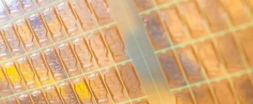
Vaso Sustratos de paquete Fabricante. Utilizamos procesos de sustrato avanzados para producir sustratos de vidrio.. El sustrato de vidrio terminado tiene una superficie más lisa.. y El material es más resistente a las altas temperaturas.. Nuestra fábrica que produce este sustrato emplea a más de 10,000 gente.
En equipos electrónicos modernos., placas de circuito impreso (PCB) se han convertido en el componente central de varios productos electrónicos. Entre los muchos tipos de PCB, Los sustratos de envases de vidrio se han vuelto cada vez más prominentes.. Como ingeniero de PCB, Una comprensión profunda de los procesos detrás de los fabricantes de sustratos de envases de vidrio es crucial para comprender las tendencias de desarrollo de la industria electrónica.. A medida que la tecnología continúa avanzando, Los sustratos de embalaje de vidrio se utilizarán cada vez más en aplicaciones electrónicas de alto rendimiento y alta confiabilidad.. ,
¿Qué es un sustrato de embalaje de vidrio??
El sustrato para envases de vidrio es un sustrato electrónico de alto rendimiento basado en sustrato de vidrio., que juega un papel clave en la industria electrónica. En comparación con los PCB tradicionales basados en sustratos orgánicos (como el FR-4), Los sustratos de embalaje de vidrio tienen mejor rendimiento y confiabilidad., y son especialmente adecuados para alta frecuencia, aplicaciones de alta velocidad y alta densidad.
En sustratos de envases de vidrio., El sustrato de vidrio se utiliza como aislamiento eléctrico y soporte mecánico., mientras que la capa de metalización (generalmente cobre) se utiliza para formar el patrón del circuito. Una de las ventajas de los sustratos de vidrio es su baja pérdida dieléctrica y su constante dieléctrica estable., lo que los hace excelentes en aplicaciones de alta frecuencia. Además, el sustrato de vidrio también tiene excelentes propiedades de conductividad térmica, lo que ayuda a disipar el calor y mantener el funcionamiento estable del circuito.
Por su excelente rendimiento y confiabilidad., Los sustratos de embalaje de vidrio se utilizan ampliamente en diversos campos., incluyendo comunicaciones, médico, aeroespacial, etc.. En el campo de las comunicaciones, Los sustratos de embalaje de vidrio se utilizan a menudo para fabricar radiofrecuencia de alto rendimiento. (RF) y circuitos de microondas para soportar la transmisión de datos de alta velocidad y la eficiencia espectral de los dispositivos de comunicación inalámbrica. En dispositivos médicos, Los sustratos de embalaje de vidrio se utilizan para fabricar equipos de monitoreo de signos vitales y sistemas de imágenes médicas., donde su estabilidad y confiabilidad son críticas para la salud y seguridad del paciente. En el campo aeroespacial, Los sustratos de embalaje de vidrio se utilizan ampliamente en las comunicaciones por satélite., sistemas de navegación y control, y su alto rendimiento y durabilidad pueden cumplir con los requisitos de entornos extremos.
En general, como de alto rendimiento, sustrato electrónico de alta confiabilidad, El sustrato de vidrio para envases desempeña un papel insustituible en los equipos electrónicos modernos., Proporcionar soporte técnico clave y soluciones para diversos campos de aplicación..
Cómo diseñar un sustrato de embalaje de vidrio?
El diseño de sustratos de envases de vidrio es una tarea de ingeniería integral que requiere que los ingenieros consideren múltiples factores para garantizar el rendimiento., estabilidad, y confiabilidad del producto final. Los siguientes son factores clave a considerar al diseñar sustratos de envases de vidrio:
El diseño del circuito es una de las primeras consideraciones en el proceso de diseño.. Los ingenieros deben organizar los componentes y las conexiones del circuito para minimizar la interferencia de la señal y el acoplamiento cruzado.. Optimizando el diseño, Se pueden reducir los retrasos en la transmisión de la señal y se puede mejorar la velocidad y el rendimiento del circuito..
En PCB multicapa, El diseño de las conexiones entre capas es crucial.. Los ingenieros deben determinar las mejores rutas para las líneas de señal y de energía y adoptar técnicas apropiadas de conexión entre capas., como por ejemplo agujeros pasantes (a través de) o vias ciegas (ciego vía), Para garantizar la estabilidad y fiabilidad de la transmisión de señales..
Es necesario considerar las cuestiones de gestión de energía durante el proceso de diseño.. Una gestión razonable del consumo de energía puede prolongar la duración de la batería de los dispositivos electrónicos, reducir la generación de calor, y mejorar la eficiencia del sistema. Los ingenieros pueden gestionar el consumo de energía mediante el uso de componentes de bajo consumo, optimización de diseños de fuentes de alimentación, e implementar modos de suspensión.
Interferencia electromagnética (EMI) e interferencias de radiofrecuencia (RFI) Son problemas comunes en el diseño de equipos electrónicos.. Para suprimir la interferencia EMI/RFI, Los ingenieros deben tomar una serie de medidas., incluido el uso de cubiertas protectoras, diseño de cable de tierra, Filtros y métodos de cableado adecuados., Para garantizar la compatibilidad electromagnética y la estabilidad del rendimiento del equipo..
La utilización de software de diseño avanzado y herramientas de simulación es clave para diseñar sustratos de envases de vidrio.. Estas herramientas pueden ayudar a los ingenieros a optimizar el cableado, Simulación de señales y análisis de compatibilidad electromagnética para garantizar la precisión y confiabilidad de las soluciones de diseño.. Al considerar exhaustivamente factores como el diseño del circuito, conexiones entre capas, gestión del consumo de energía, y supresión de EMI/RFI, Los ingenieros pueden diseñar sustratos de envases de vidrio con un rendimiento excelente., Estabilidad y confiabilidad para satisfacer las necesidades de diferentes escenarios de aplicación..
¿Cuál es el proceso de fabricación de sustratos de envases de vidrio??
El proceso de fabricación de sustratos de envases de vidrio es un proceso complejo y preciso que requiere un diseño cuidadoso y un control estricto.. El siguiente es el proceso de fabricación detallado.:
El primer paso en la fabricación de un sustrato de embalaje de vidrio es preparar los materiales necesarios.. El primero es seleccionar sustratos de vidrio de alta calidad., que debe tener un espesor constante y superficies planas para garantizar la estabilidad y confiabilidad del circuito.. Además, se requieren otros materiales, como materiales de metalización (como cobre o plata), materiales dieléctricos (como películas de poliimida), y materiales de soldadura.
Una vez que los materiales estén listos, el siguiente paso es convertir el diseño gráfico del circuito en un archivo CAD. En esta etapa, Los ingenieros utilizan software CAD para dibujar gráficos de circuitos y realizar el cableado y la disposición para garantizar el rendimiento y la confiabilidad del circuito.. La calidad del diseño gráfico afecta directamente a la calidad y rendimiento del producto final..
Una vez finalizado el diseño gráfico., el archivo CAD se transfiere a la superficie del sustrato mediante tecnología de fotolitografía. Este paso implica el uso de fotoprotector para transferir el patrón del circuito a una máscara que cubre la superficie de un sustrato de vidrio.. Luego, el patrón se transfiere a la superficie del sustrato mediante un proceso de exposición y desarrollo., Crear un patrón que pueda usarse para hacer circuitos..
Después de transferir el patrón, el siguiente paso es depositar metal u otros materiales en la superficie del sustrato para formar el patrón del circuito.. Esto generalmente se logra mediante técnicas como la deposición química de vapor. (ECV) o deposición física de vapor (PVD). Después de la deposición del metal, pasos como la fotolitografía, aguafuerte, Se requieren limpieza y limpieza para eliminar el material no deseado y formar el patrón del circuito final..
Una vez completada la deposición, Se utilizan métodos químicos o mecánicos para eliminar el material no deseado y formar el patrón del circuito final.. Este proceso se llama grabado., y suele utilizar técnicas de grabado húmedo o seco.. Una vez completado el grabado, Se requieren limpieza e inspección para garantizar la calidad y precisión del patrón del circuito..
El último paso crítico es la inspección y prueba rigurosas del sustrato fabricado para garantizar que cumpla con las especificaciones y requisitos de calidad.. Esto incluye inspección visual, Mediciones dimensionales, pruebas eléctricas y pruebas de confiabilidad, etc.. Sólo después de pasar estrictas inspecciones y pruebas se puede entregar el sustrato a los clientes y utilizarlo en la producción y montaje de dispositivos electrónicos..
A través de los pasos anteriores, Los fabricantes de sustratos de embalaje de vidrio pueden producir alta calidad., Sustratos electrónicos de alto rendimiento para satisfacer las necesidades de diversos campos de aplicación y brindar a los clientes soluciones confiables..
¿Cuánto cuesta un sustrato de embalaje de vidrio??
Cuando consideramos el costo de los sustratos de embalaje de vidrio, hay muchos factores a considerar, incluyendo procesos de fabricación, selección de material, requisitos de especificación, y cantidades de pedido. Profundicemos en estos factores para comprender mejor la estructura de costos de los sustratos de embalaje de vidrio..
En primer lugar, El proceso de fabricación es uno de los factores importantes que afectan el costo de los sustratos de embalaje de vidrio.. Los procesos de fabricación avanzados suelen requerir más inversión en tecnología y equipos., entonces el costo será relativamente alto. Por ejemplo, si el proceso de fabricación requiere el uso de técnicas complejas de fotolitografía o pasos de procesamiento químico especiales, los costos aumentarán en consecuencia.
En segundo lugar, La selección de materiales también tiene un impacto importante en el costo.. Los sustratos de vidrio para envases suelen requerir materiales de alta calidad, como sustratos de vidrio especiales., materiales de metalización (como cobre o plata), y materiales dieléctricos de alto rendimiento.. La elección de materiales de alta calidad puede mejorar el rendimiento y la confiabilidad del producto., pero también puede aumentar los costos de fabricación..
Además, Los requisitos de especificación también tendrán un impacto en los costos.. Los sustratos de embalaje de vidrio personalizados y de alto rendimiento normalmente deben cumplir especificaciones más estrictas., como una mayor frecuencia de operación, menor distorsión de la señal, etc.. Cumplir con estas especificaciones puede requerir pasos de proceso adicionales o materiales especiales., costos crecientes.
Finalmente, La cantidad del pedido también es un factor importante que afecta el costo.. La producción de alto volumen a menudo permite ventajas de escalamiento de costos porque los costos fijos se pueden distribuir entre una mayor cantidad de productos.. En contraste, La producción de bajo volumen suele ser más costosa porque los costos fijos se distribuyen entre un número relativamente pequeño de productos..
Para resumir, El costo de los sustratos de embalaje de vidrio se ve afectado por muchos factores., incluyendo el proceso de fabricación, selección de material, requisitos de especificación y cantidad de pedido. En general, El costo de los productos personalizados y de alto rendimiento es mayor., mientras que el costo de los productos producidos en masa con especificaciones estándar es relativamente bajo. Por lo tanto, Es muy importante que los clientes elijan el fabricante adecuado y consideren los factores de costo durante la etapa de diseño..
¿Cuál es el material del sustrato del embalaje de vidrio??
El sustrato de vidrio para envases es un componente clave de los sustratos electrónicos de alto rendimiento, y su selección de materiales es crucial. Los siguientes son los principales materiales y características de los sustratos de envases de vidrio.:
Sustrato de vidrio: El sustrato de vidrio es el material básico del sustrato de embalaje de vidrio.. Tiene una excelente planitud y planitud superficial., que puede garantizar la precisión y estabilidad del diseño del circuito. Los sustratos de vidrio suelen tener una excelente estabilidad térmica y química., Puede soportar procesos de alta temperatura y alta presión., y mantener buenas propiedades físicas y químicas.
Materiales metalizados: Revestimiento de materiales metalizados en la superficie del sustrato de vidrio., Incluyendo principalmente metales como el cobre y la plata.. Estos materiales metalizados se utilizan para formar patrones de circuitos y conectores.. Tienen buena conductividad eléctrica y resistencia a la corrosión., Y puede garantizar una transmisión estable de señales de circuito y una buena conectividad..
Material dieléctrico: El material dieléctrico suele ser una película de poliimida. (película PI), que se utiliza para cubrir y proteger capas de circuitos para evitar cortocircuitos e interferencias entre circuitos.. La película de poliimida tiene excelentes propiedades aislantes., resistencia al calor y resistencia química, que puede proteger circuitos en diversos entornos extremos y garantizar su funcionamiento estable.
Soldar: La soldadura se utiliza para soldar componentes electrónicos y conectores a la superficie de sustratos de vidrio para garantizar su conexión confiable al circuito.. Los materiales de soldadura comúnmente utilizados incluyen soldadura, aleación de plomo y estaño, etc., que tienen buen rendimiento de soldadura y resistencia mecánica y pueden garantizar la firmeza y estabilidad de la junta soldada.
Juntos, Estos materiales forman la estructura central del sustrato del embalaje de vidrio., que tiene excelente electricidad, Propiedades térmicas y mecánicas y es adecuado para diversos entornos de aplicaciones complejas.. Seleccionando y optimizando cuidadosamente estos materiales, Los fabricantes de sustratos de embalaje de vidrio pueden proporcionar alta calidad., Productos de alta confiabilidad que satisfacen a los clientes.’ diferentes necesidades y escenarios de aplicación.
¿Quién fabrica sustratos de embalaje de vidrio??
¿Quién fabrica sustratos de embalaje de vidrio?? El problema genera preocupación entre los fabricantes.. en esta zona, elegir el proveedor adecuado es crucial. Nuestra empresa es conocida por su tecnología de fabricación superior y servicio al cliente.. Como uno de los principales proveedores de sustratos de embalaje de vidrio., no somos solo su fabricante, somos tu socio.
En primer lugar, Contamos con equipos y tecnología de producción avanzados.. Nuestra fábrica está equipada con las últimas líneas de producción y equipos de procesamiento de alta precisión., capaz de cumplir con diversos requisitos complejos de fabricación de PCB. Del diseño gráfico al producto final, Adoptamos estrictos procesos de producción y medidas de control de calidad para garantizar que cada sustrato de embalaje de vidrio cumpla con los requisitos y estándares del cliente..
En segundo lugar, Contamos con un equipo profesional experimentado.. Nuestros ingenieros y técnicos tienen muchos años de experiencia y conocimientos en la industria y pueden brindar a los clientes soluciones y soporte técnico integral.. Ya sea en la fase de diseño o durante la producción, Podemos proporcionar a los clientes servicios personalizados para satisfacer sus necesidades y requisitos específicos..
Además de esto, También nos centramos en la experiencia y satisfacción del cliente.. Siempre ponemos a los clientes primero, adherirse a la filosofía empresarial de “integridad, calidad, servicio” y esforzarnos por crear mayor valor para los clientes. Ya sea en términos de ciclo de entrega de pedidos o servicio posventa, Nos esforzamos por hacer nuestro mejor esfuerzo para garantizar la satisfacción y lealtad del cliente..
Finalmente, Ofrecemos a nuestros clientes productos y servicios de la más alta calidad a precios competitivos y métodos de entrega flexibles.. Sabemos que el control de costes es crucial para nuestros clientes., por eso no solo nos centramos en la calidad del producto, sino también en la competitividad de precios. Estamos comprometidos a brindar a los clientes las soluciones más rentables para ayudarlos a lograr un mayor éxito en el mercado..
Para resumir, como fabricante profesional de sustratos de vidrio para envases, nuestra empresa tiene una rica experiencia, tecnología avanzada y servicios de alta calidad, que puede satisfacer las diversas necesidades de los clientes y crear mayor valor y éxito para ellos.. Elíjanos, elija confianza y garantía de calidad.
¿Cuáles son los 5 cualidades de un excelente servicio al cliente?
Un excelente servicio al cliente es crucial para los fabricantes de PCB. Aquí están 5 cualidades de un excelente servicio al cliente:
Sensibilidad: En la industria electrónica, el tiempo es dinero. Un excelente servicio al cliente significa respuestas rápidas a las consultas y preguntas de los clientes.. Respondiendo rápidamente a las necesidades del cliente, Los fabricantes pueden establecer canales de comunicación eficientes para garantizar que los clientes reciban soporte y soluciones oportunas.. Ya sea consulta sobre problemas técnicos o seguimiento de pedidos, La respuesta rápida puede mejorar la confianza del cliente y mejorar su satisfacción..
Conocimiento profesional: En el campo de la fabricación de PCB, El conocimiento profesional es uno de los pilares de la competitividad de los fabricantes.. Un excelente equipo de servicio al cliente debe tener una rica experiencia en la industria y conocimientos profesionales y ser capaz de brindar a los clientes sugerencias y soporte técnico precisos y efectivos.. Si los clientes enfrentan desafíos de diseño, Problemas con la selección de materiales o el proceso de producción., Un equipo con conocimientos profesionales puede proporcionar a los clientes las soluciones más adecuadas y ayudarlos a alcanzar los objetivos del proyecto..
Servicios personalizados: Cada cliente tiene sus propias necesidades y requisitos únicos., por lo que los servicios personalizados son cruciales para los fabricantes de PCB. Un excelente equipo de atención al cliente debería poder proporcionar soluciones personalizadas basadas en los clientes.’ necesidades específicas, Asegurar que los productos cumplan con los requisitos y expectativas del cliente.. Ya sea un diseño personalizado para un campo de aplicación específico o la necesidad de materiales y procesos especiales, Los fabricantes deben responder con flexibilidad para satisfacer las necesidades individuales de los clientes..
Seguro de calidad: En la industria electrónica, La calidad del producto es clave para que los fabricantes se ganen la confianza y la reputación del cliente.. Por lo tanto, Un excelente equipo de servicio al cliente debe implementar estrictamente el sistema de gestión de calidad para garantizar que la calidad del producto sea estable y confiable y cumpla con los requisitos y estándares del cliente.. Desde la adquisición de materia prima hasta la producción y fabricación hasta la entrega final., Los fabricantes deben realizar inspecciones y controles de calidad estrictos para garantizar que cada lote de productos cumpla con los más altos estándares de calidad..
Soporte postventa: Un excelente servicio al cliente incluye no solo el servicio durante el proceso de venta., sino también soporte y servicio postventa. Los fabricantes deben proporcionar un soporte postventa integral, incluida la formación técnica, mantenimiento y solucion de problemas, Para garantizar que los clientes puedan recibir ayuda y soporte oportunos durante el uso.. Estableciendo un sólido sistema de servicio postventa, Los fabricantes pueden mejorar la satisfacción y lealtad del cliente y promover el establecimiento de relaciones de cooperación a largo plazo..
Para resumir, Un excelente servicio al cliente es crucial para los fabricantes de PCB.. A través de las cinco características de la respuesta rápida, conocimiento profesional, servicios personalizados, Garantía de calidad y soporte postventa., Los fabricantes pueden mejorar la satisfacción del cliente., obtener ventajas competitivas en el mercado, y lograr el desarrollo sostenible.
Preguntas frecuentes
¿Para qué áreas de aplicación son adecuados los sustratos de envases de vidrio??
Los sustratos para envases de vidrio son sustratos electrónicos versátiles que se utilizan ampliamente en muchas áreas de aplicación diferentes.. Estos incluyen, entre otros, tecnología de la comunicación., equipo medico, aeroespacial, aplicaciones militares y sistemas de control industrial, etc.. Por su excelente rendimiento eléctrico, rendimiento térmico y confiabilidad, Los sustratos de embalaje de vidrio son especialmente adecuados para aplicaciones con requisitos de alto rendimiento para alta frecuencia., Circuitos de alta velocidad y alta densidad..
¿Cuál es el tamaño máximo de un sustrato de embalaje de vidrio??
El tamaño de un sustrato de embalaje de vidrio suele estar limitado por el proceso y el equipo de fabricación., por lo que su tamaño máximo variará de un fabricante a otro. Sin embargo, Las modernas técnicas de fabricación han permitido la producción de sustratos de envases de vidrio de tamaño considerable., a menudo alcanza tamaños de decenas de centímetros. Para requisitos de tamaño especialmente grandes, La fabricación personalizada puede ser una mejor opción..
¿Cuánto dura el ciclo de producción de sustratos de envases de vidrio??
El plazo de producción de sustratos de envases de vidrio depende de muchos factores, incluyendo las capacidades de producción del fabricante, el tamaño y la complejidad del pedido, y requisitos específicos del cliente. En general, Los plazos de producción suelen oscilar entre días y semanas., pero puede ser más largo para proyectos particularmente complejos o personalizados. Al determinar los plazos de producción, Los fabricantes a menudo trabajan en estrecha colaboración con los clientes para garantizar que se cumplan los requisitos de tiempo del cliente..
¿Cuál es la diferencia entre el sustrato de vidrio para envases y el sustrato tradicional FR-4??
Los sustratos de vidrio para envases tienen algunas diferencias significativas en comparación con los sustratos FR-4 tradicionales.. En primer lugar, Los sustratos de embalaje de vidrio generalmente utilizan sustratos de vidrio como material base., mientras que los sustratos FR-4 utilizan resina epoxi reforzada con fibra de vidrio. En segundo lugar, el sustrato de embalaje de vidrio tiene un mejor rendimiento de alta frecuencia y rendimiento térmico, y es adecuado para aplicaciones de alta frecuencia y alta velocidad. Además, El proceso de fabricación de sustratos de envases de vidrio también es más complejo y el coste suele ser mayor., pero tiene más ventajas en algunas aplicaciones con mayores requisitos de rendimiento.
¿El diseño de sustratos de envases de vidrio requiere consideraciones especiales??
Sí, Hay algunos factores que requieren especial atención al diseñar sustratos de envases de vidrio.. Por la particularidad de sus materiales y procesos de fabricación., Los sustratos de embalaje de vidrio son diferentes de los sustratos FR-4 tradicionales en términos de diseño del circuito., conexiones entre capas, Gestión del consumo de energía y supresión de EMI/RFI.. Por lo tanto, Es necesario trabajar en estrecha colaboración con ingenieros de diseño de PCB profesionales durante la etapa de diseño para garantizar la estabilidad., La confiabilidad y el rendimiento del diseño del circuito cumplen con los requisitos del cliente..