CO., LTD")
Proveedor de PCB multicapa con alto TG. FR4 TG 170. TG 180. TG200. TG 260, TG 280, placas pcb de alta calidad. y un precio más barato. Producimos placas PCB de 2 capa a 50 capa. ahorra tu dinero y tu tiempo.
Hemos utilizado base FR4. AL base. base de cobre. Base flexible. Base rígida-flexible. base rogers. y otros tipos de núcleo base de PCB.
PCB MULTICAPA DE ALTO TG
En el mundo de la electrónica., placas de circuito impreso (PCB) son la columna vertebral de la tecnología moderna, Permitir que funcionen los innumerables dispositivos en los que confiamos a diario.. Entre los muchos tipos de PCB, Los PCB multicapa de alto TG destacan por su rendimiento superior y durabilidad en aplicaciones exigentes. Esta guía completa profundiza en las complejidades de los PCB multicapa con alto TG, cubriendo todo, desde principios de diseño hasta procesos de fabricación y consideraciones de costos..
¿Qué es la PCB multicapa con alto TG??
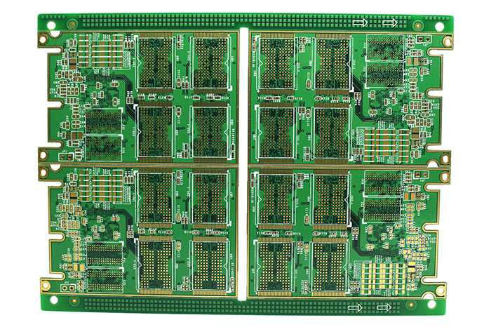
PCB multicapa de alto TG (PCB multicapa de alto TG) es un tipo especial de placa de circuito impreso (tarjeta de circuito impreso) Ampliamente utilizado en el campo de la electrónica moderna.. En comparación con los PCB ordinarios, Los PCB multicapa con alto TG tienen mayor resistencia al calor y estabilidad en entornos de alta temperatura., y son adecuados para escenarios de aplicación con requisitos de alta temperatura ambiente. Presentan una estructura de sustrato multicapa., A menudo se utiliza una temperatura de transición vítrea alta. (TG) Materiales de sustrato como FR-4 para garantizar un rendimiento eléctrico estable en condiciones de temperatura extrema..
La PCB multicapa con alto TG tiene muchas características y ventajas importantes. Primero, Tienen una alta estabilidad térmica y pueden funcionar en entornos de alta temperatura durante largos períodos de tiempo sin fallar., lo que los hace particularmente adecuados para equipos electrónicos de alta temperatura o aplicaciones que requieren operación a largo plazo en ambientes de alta temperatura. En segundo lugar, PCB multicapa de alto TG tiene excelente resistencia mecánica y resistencia al impacto., y puede mantener conexiones de circuito estables en entornos de trabajo hostiles, Reducir el riesgo de daños en el circuito debido al estrés mecánico.. Además, La PCB multicapa con alto TG también tiene buena resistencia a la corrosión química y excelentes propiedades eléctricas., Asegurar que la placa de circuito pueda funcionar de manera confiable en diversas condiciones ambientales..
Además de las características anteriores, PCB multicapa con alto TG también tiene un buen rendimiento de soldadura y rendimiento de procesamiento, facilitando su fabricación e instalación. Se pueden utilizar en diversos campos de aplicación., incluyendo equipo de comunicación, sistemas de control industriales, electrónica automotriz, equipo medico, etc., Proporcionar conexiones de circuitos confiables y un rendimiento estable para productos en estos campos..
En general, PCB multicapa de alto TG tiene una posición importante y amplias perspectivas de aplicación en el campo electrónico moderno. Su excelente rendimiento y estabilidad proporcionan soluciones confiables para diversos escenarios de aplicación.. Con el continuo avance de la tecnología y la creciente demanda del mercado, El desarrollo de PCB multicapa con alto TG seguirá recibiendo atención y desempeñará un papel más importante en el futuro..
Cómo diseñar PCB multicapa de alto TG?
El diseño de una PCB multicapa con alto TG es una tarea compleja y crítica que requiere la consideración de múltiples factores para garantizar el rendimiento y la confiabilidad del producto final.. Los siguientes son los factores clave y los principios de diseño a considerar al diseñar PCB multicapa con alto TG:
Gestión térmica: Los PCB multicapa con alto TG se utilizan a menudo en entornos de alta temperatura., por lo que la gestión térmica es una consideración clave durante el proceso de diseño. El diseño razonable de disipación de calor puede reducir efectivamente la temperatura de la placa de circuito y mejorar la estabilidad y vida útil del sistema..
Integridad de señal: Mantener la integridad de la señal es un punto crítico en el proceso de diseño.. El cableado razonable y el control de impedancia pueden reducir la distorsión de la señal y la diafonía., Garantizar una transmisión de señal estable en aplicaciones de alta velocidad y alta frecuencia..
Compatibilidad electromagnética (CEM): Es necesario considerar la reducción de la interferencia electromagnética y la mejora de las capacidades antiinterferencias en el diseño para cumplir con los requisitos de compatibilidad electromagnética.. Un buen diseño y diseño de blindaje pueden reducir eficazmente la radiación electromagnética y la interferencia de señales sensibles..
Estabilidad mecánica: La estabilidad mecánica de los PCB afecta directamente a su fiabilidad durante su uso.. La conexión razonable entre capas y el diseño de la estructura de soporte pueden garantizar la estabilidad de la PCB en condiciones de vibración e impacto..
Selección de material: Seleccionar materiales con alto TG adecuados para ambientes de alta temperatura es una decisión importante en el proceso de diseño.. Estos materiales tienen altas temperaturas de transición vítrea., que garantizan la estabilidad y confiabilidad de las placas de circuito en ambientes de alta temperatura.
Diseño de embalaje y disipación de calor.: La selección adecuada del embalaje y el diseño de disipación de calor pueden reducir eficazmente la temperatura de funcionamiento de los componentes electrónicos y mejorar el rendimiento y la vida útil del sistema..
Grosor y número de capas.: Elija el espesor y el número de capas adecuados según los requisitos de diseño y los escenarios de aplicación.. El grosor apropiado de la placa y el diseño del número de capas pueden cumplir con los requisitos de diseño del circuito y disipación de calor mientras se mantiene la estabilidad mecánica de la placa de circuito..
Verificación del diseño: La simulación y la verificación son fundamentales durante el proceso de diseño.. Simule el rendimiento del circuito y las características térmicas con herramientas de simulación., y verificar que los diseños cumplan con los requisitos esperados con prototipos.
Cumplir con estándares y especificaciones.: Se deben seguir los estándares y especificaciones relevantes de la industria durante el proceso de diseño para garantizar que la PCB multicapa de alto TG diseñada cumpla con los requisitos de seguridad y confiabilidad..
Comunicación con los fabricantes.: Mantener una comunicación estrecha con los fabricantes de PCB y obtener comentarios y sugerencias oportunos.. Los fabricantes pueden proporcionar soporte técnico valioso para ayudar a optimizar los diseños y resolver problemas potenciales..
El diseño de PCB multicapa con alto TG requiere una consideración exhaustiva de los factores anteriores y el cumplimiento de los principios de diseño correspondientes para garantizar que el producto final funcione bien en entornos exigentes y de alta temperatura y satisfaga las necesidades y expectativas del cliente..
¿Cuál es el proceso de fabricación de PCB multicapa con alto TG??
El proceso de fabricación de PCB multicapa de alto TG es un proyecto preciso y complejo que involucra múltiples pasos críticos para garantizar que el producto final tenga un excelente rendimiento y confiabilidad.. El proceso de fabricación de PCB multicapa con alto TG se presentará en detalle a continuación..
Primero, El proceso de fabricación de PCB multicapa de alto TG comienza con la preparación de los archivos de diseño.. Los archivos de diseño suelen ser creados por ingenieros de circuitos utilizando un software de diseño de PCB profesional., que incluyen información de diseño, como el diseño del circuito., rutas de cableado, colocación de componentes, etc..
Lo siguiente es la preparación del material del sustrato.. Los PCB multicapa con alto TG suelen utilizar materiales de sustrato con temperaturas de transición vítrea más altas. (valores de TG), como el FR-4, para garantizar la estabilidad y confiabilidad en entornos de alta temperatura. Estos materiales de sustrato deben pasar por pasos de preprocesamiento, como corte y limpieza, para garantizar que la superficie sea plana y limpia..
Luego están los gráficos.. Determinar el diseño del circuito y los métodos de conexión en cada nivel mediante la visualización gráfica de los archivos de diseño es uno de los pasos clave en la fabricación de PCB multicapa con alto TG.. El patrón del circuito se transfiere a la superficie del sustrato mediante tecnología de fotolitografía para formar el patrón del circuito..
Luego viene la perforación. Utilice una máquina perforadora de alta precisión para perforar agujeros en el sustrato para prepararlo para las conexiones y soldaduras posteriores entre capas.. La precisión y exactitud posicional de la perforación son fundamentales para la calidad del producto final..
Luego vienen las capas. en este paso, Se superponen múltiples sustratos perforados y se utiliza adhesivo para unirlos de forma segura.. El proceso de laminación requiere un alto grado de precisión y estabilidad para garantizar que las conexiones eléctricas y la resistencia mecánica entre las diferentes capas cumplan los requisitos..
Luego viene la deposición y el modelado de la lámina de cobre.. Se deposita una lámina de cobre sobre la superficie del sustrato y se modela mediante fotolitografía para formar caminos conductores para el patrón del circuito.. Este paso es uno de los pasos clave en la fabricación de circuitos de PCB y determina el rendimiento conductivo y la estabilidad del circuito..
Luego viene el grabado. Las partes no cubiertas por la lámina de cobre se eliminan mediante grabado químico para formar el patrón del circuito final.. El proceso de grabado requiere un control estricto de la concentración y temperatura de la solución química para garantizar la precisión y consistencia del grabado..
El último paso es aplicar una capa protectora.. Proteja el patrón del circuito del ambiente externo y aumente la resistencia mecánica y la durabilidad del circuito aplicando una capa protectora. (como película de soldadura). El proceso de recubrimiento requiere un espesor de recubrimiento uniforme y estable para garantizar que el rendimiento de la capa protectora cumpla con los requisitos..
En resumen, El proceso de fabricación de PCB multicapa con alto contenido de TG implica varios pasos clave., incluyendo la preparación del archivo de diseño, preparación del material del sustrato, modelado, perforación, laminación, Deposición y modelado de láminas de cobre., aguafuerte, y el recubrimiento de capas protectoras espera. Cada paso requiere un control preciso del proceso y una gestión de la calidad para garantizar que el rendimiento y la confiabilidad del producto final cumplan con los requisitos de diseño..
Cómo fabricar PCB multicapa de alto TG?
La fabricación de PCB multicapa con alto TG es un proceso complejo y preciso que involucra múltiples pasos y enlaces clave.. Los siguientes son los pasos específicos para la fabricación de PCB multicapa con alto TG y los aspectos clave a los que se debe prestar atención.:
Antes de entrar oficialmente en la etapa de fabricación., Primero se debe verificar el diseño de la PCB para garantizar el cumplimiento de las especificaciones y requisitos de diseño.. Esto incluye revisión y verificación de los documentos de diseño y preparación de los materiales y equipos necesarios..
Seleccione un material de sustrato con alto TG (como el FR-4) y lámina de cobre adecuada, y diseñar la estructura apilada de acuerdo con los requisitos de diseño. En esta etapa, factores como el número de capas de PCB, espesor del material, y se debe considerar el espesor de la lámina de cobre.
Convierta archivos de diseño de PCB en archivos de imágenes gráficas (Archivos Gerber). Estos archivos contienen información clave, como el cableado., ubicaciones de componentes, y ubicaciones de perforación para cada capa.
Se utiliza una máquina CNC para cortar el material del sustrato al tamaño requerido y perforar orificios en ubicaciones predeterminadas para preparar el cableado y el montaje de componentes..
La lámina de cobre del tablero de la capa interior está cubierta sobre el sustrato., y luego el tablero de la capa interna y la lámina de cobre se unen para formar una estructura multicapa mediante procesos como el prensado en caliente y el tratamiento químico..
Usando tecnología de fotolitografía, Los gráficos del archivo Gerber se reproducen en el tablero de la capa interna y en la lámina de cobre para formar patrones conductores y ubicaciones de componentes..
Utilice tecnología de grabado químico para eliminar láminas de cobre innecesarias y exponer las rutas conductoras requeridas., y luego aplicar una capa protectora (máscara de soldadura, capa revestida de cobre, etc.) Para proteger la superficie de la PCB y lograr funciones específicas..
Los paneles exteriores se apilan encima de los paneles interiores y se unen mediante calor y presión.. Luego se lleva a cabo el procesamiento y procesamiento final., incluido el recorte de bordes, alisado de superficies, etc..
La PCB fabricada se somete a rigurosas pruebas eléctricas., incluyendo pruebas de conectividad, prueba de resistencia de aislamiento, etc., para garantizar que cumple con las especificaciones de diseño y tiene un buen rendimiento eléctrico. Al mismo tiempo, Se lleva a cabo un control de calidad para garantizar que cada enlace cumpla con los estándares y requisitos..
En el proceso de fabricación de PCB multicapa con alto TG, Los enlaces clave incluyen la selección de materiales., diseño de estructura apilada, imágenes gráficas, procesamiento químico y pruebas eléctricas. Solo siguiendo estrictamente cada paso y garantizando el control de calidad se pueden producir productos de PCB multicapa con alto TG que cumplan con altos estándares..
¿Cuáles son las consideraciones de costo para los PCB multicapa con alto TG??
El costo de los PCB multicapa con alto TG está determinado por una variedad de factores, que afectan directamente el nivel de los costos de fabricación. Comprender estos factores puede ayudar a los fabricantes e ingenieros de diseño a optimizar los costos sin comprometer la calidad..
En primer lugar, El tamaño y el número de capas de la PCB son uno de los factores clave que afectan el costo.. En general, Un tamaño más grande y más capas de PCB aumentarán el costo de fabricación.. Esto se debe a que se requieren más materiales y pasos de procesamiento., lo que lleva a mayores costos. Para reducir costos, Puede considerar optimizar el diseño y reducir el tamaño y la cantidad de capas de la PCB para cumplir con los requisitos del producto y al mismo tiempo reducir los costos de fabricación..
En segundo lugar, La complejidad del diseño de PCB también afectará el costo.. El diseño complejo y el enrutamiento de circuitos pueden requerir más pasos de procesamiento y requisitos técnicos más altos., aumentando así los costos de fabricación. Por lo tanto, El diseño debe simplificarse tanto como sea posible durante la etapa de diseño para reducir la complejidad innecesaria y reducir los costos de fabricación..
La selección de materiales también es un factor importante que afecta el costo.. Los materiales con alto TG son generalmente más caros que los materiales FR-4 normales., pero ofrecen mayor estabilidad térmica y confiabilidad. En algunos escenarios de aplicación, es necesario el uso de materiales con alto TG, pero en algunas situaciones donde no se requiere estabilidad a altas temperaturas, Se pueden considerar materiales más económicos para reducir costos..
Además, Los requisitos del proceso de fabricación de PCB también tendrán un impacto en los costos.. Algunos requisitos de proceso especiales, como la impedancia controlada, requisitos especiales de tratamiento de superficies, etc., puede requerir pasos de procesamiento adicionales y requisitos técnicos más altos, aumentando así los costos de fabricación. Se deben evitar requisitos de proceso demasiado complejos durante la etapa de diseño para reducir costos..
Finalmente, El volumen de producción también es uno de los factores que afecta los costos.. En general, La producción en masa puede reducir el costo de fabricación de un producto unitario porque los costos de material y mano de obra se pueden ahorrar mediante la producción a gran escala.. Por lo tanto, El volumen de producción debe considerarse plenamente durante la etapa de planificación del proyecto para lograr una mejor rentabilidad..
En general, El costo de fabricación de PCB multicapa con alto TG se ve afectado por muchos factores., incluido el tamaño y el número de capas, complejidad del diseño, selección de material, requisitos del proceso, y volumen de producción. Estos factores deben considerarse de manera integral durante las etapas de diseño y fabricación., y se deben tomar medidas efectivas para reducir los costos y al mismo tiempo garantizar la calidad y el rendimiento del producto..
¿Qué materiales se utilizan en PCB multicapa con alto TG??
PCB multicapa High TG es una placa de circuito impreso con excelente rendimiento y confiabilidad en ambientes de alta temperatura., y su selección de materiales es crucial. Típicamente, Los materiales clave utilizados en los PCB multicapa con alto TG incluyen materiales de sustrato., lámina de cobre, revestimientos de almohadillas y revestimientos de superficies. Las siguientes son las características de estos materiales y su papel en la fabricación de PCB.:
El material de sustrato de PCB multicapa con alto TG generalmente usa FR-4 (Retardante de llama No. 4) Resina epoxi reforzada con fibra de vidrio con una temperatura de transición vítrea más alta. (valor de TG). FR-4 tiene excelentes propiedades de aislamiento, resistencia mecánica y resistencia al calor, y puede mantener un rendimiento estable en entornos de alta temperatura, haciéndolo adecuado para aplicaciones que requieren tolerancia a altas temperaturas.
La lámina de cobre es el material de la capa conductora de PCB multicapa de alto TG y se utiliza para formar patrones de circuitos y rutas conductoras.. Los espesores de lámina de cobre comunes incluyen 1 oz, 2onz, y 3 onzas, que se seleccionan en función de los requisitos actuales y las necesidades de disipación de calor de la placa de circuito. La lámina de cobre tiene buena conductividad eléctrica y procesabilidad., y puede cumplir con los complejos requisitos de diseño de PCB multicapa.
El revestimiento de la almohadilla suele estar compuesto de una aleación de estaño. (sn) y liderar (Pb), y también puede ser soldadura sin plomo. Estos recubrimientos cubren la superficie de la almohadilla de la PCB y se utilizan para soldar componentes.. El recubrimiento adecuado de la almohadilla puede proporcionar un buen rendimiento de soldadura y garantizar una conexión de soldadura fuerte y confiable..
El revestimiento de superficie se utiliza para proteger las almohadillas y los cables de la PCB., prevenir la oxidación y la corrosión, y proporciona un buen rendimiento de soldadura. Los revestimientos de superficies comunes incluyen HASL (soldadura de aire caliente), Aceptar (galvanoplastia de oro), OSP (protección química orgánica) y Plata de Inmersión (plata de inmersión). La elección del revestimiento de superficie adecuado depende del escenario de aplicación de PCB, Requisitos medioambientales y proceso de soldadura..
Para resumir, Los materiales clave de la PCB multicapa con alto TG tienen un rendimiento y características excelentes y pueden cumplir con los requisitos de trabajo en condiciones duras, como altas temperaturas., alta presión y alta frecuencia. La selección y el uso adecuados de estos materiales pueden garantizar la estabilidad., Fiabilidad y rendimiento a largo plazo de los PCB., promoviendo así el desarrollo y la innovación de productos electrónicos..
¿Quiénes son los principales fabricantes de PCB multicapa con alto contenido de TG??
En el campo de la fabricación de PCB multicapa con alto TG, Algunos fabricantes importantes se han convertido en líderes de la industria con su excelente solidez técnica y su rica experiencia.. Entre ellos, como empresa líder centrada en la fabricación de PCB de alta calidad, Nuestra empresa tiene una influencia y reputación significativas en este campo..
Nuestra empresa se compromete a proporcionar a los clientes soluciones de PCB multicapa con alto TG. Las características de su producto son las siguientes.:
Excelente control de calidad: Nuestra empresa se basa en estrictos procesos de control de calidad para garantizar que cada PCB multicapa con alto TG producido cumpla con los más altos estándares.. Desde la adquisición de materia prima hasta la entrega final, Cada proceso es cuidadosamente monitoreado e inspeccionado para garantizar la consistencia y confiabilidad de la calidad del producto..
Tecnología de fabricación avanzada: La empresa cuenta con equipos de producción avanzados y equipos técnicos., que puede responder de manera flexible a diversos requisitos de diseño complejos y desafíos de procesamiento. Introduciendo la última tecnología y procesos de fabricación., Nos aseguramos de que se optimicen la eficiencia de producción y el nivel de calidad de los PCB multicapa con alto contenido de TG..
Servicios personalizados: La empresa se centra en trabajar estrechamente con los clientes para comprender sus necesidades y ofrecer soluciones personalizadas.. Ya sea para requisitos de campo de aplicación específicos o necesidades de diseño especiales, Nuestra empresa es capaz de proporcionar servicios personalizados flexibles para satisfacer las necesidades individuales de los clientes..
Cadena de suministro estable: Como fabricante de PCB de buena reputación, Nuestra empresa ha establecido un sistema de cadena de suministro estable y confiable para garantizar el suministro oportuno de materias primas y la continuidad de la producción del producto.. Esto permite a los clientes confiar con confianza en los productos de alta calidad proporcionados por la empresa y garantiza el buen progreso de sus proyectos..
Para resumir, como uno de los principales fabricantes de PCB multicapa con alto TG, Nuestra empresa se ha ganado la confianza y los elogios de los clientes con su excelente calidad., tecnología avanzada y servicios personalizados. Ya sea en el campo de las comunicaciones electrónicas, control industrial o equipo médico, Nuestra empresa puede proporcionar a los clientes soluciones confiables de PCB multicapa con alto TG para ayudarlos a lograr lanzamientos exitosos de productos y mejorar la competitividad en el mercado..
¿Cuáles son las cinco cualidades de un excelente servicio al cliente??
Un excelente servicio al cliente es un componente clave para el éxito de cualquier negocio.. No se trata sólo de responder a los clientes’ dudas o resolver sus quejas, se trata más de construir relaciones a largo plazo y mejorar la satisfacción del cliente.. Aquí hay cinco rasgos clave y lo que puede hacer para lograr un excelente servicio al cliente.:
El atributo número uno de un excelente servicio al cliente es la respuesta rápida a las necesidades y preguntas de los clientes.. Esto incluye responder rápidamente a los correos electrónicos., Llamadas telefónicas o chats en línea y resolución de problemas de los clientes en el menor tiempo posible.. Para lograr esto, Las empresas pueden mejorar la capacidad de respuesta capacitando a los empleados y adoptando sistemas y flujos de trabajo automatizados..
La honestidad y la transparencia son claves para generar confianza en el cliente. Las empresas deben proporcionar información precisa y evitar exagerar u ocultar detalles importantes.. La transparencia también significa notificar rápidamente a los clientes cuando surgen problemas y brindar soluciones honestas.. Establecer canales de comunicación transparentes, tales como mecanismos de retroalimentación de los clientes y procesos de manejo de quejas de los clientes., puede ayudar a las empresas a lograr integridad y transparencia.
Un excelente servicio al cliente requiere buenas habilidades profesionales y conocimiento de la industria.. Los empleados deben estar bien capacitados., familiarizado con los productos y servicios de la empresa, y capaz de proporcionar información precisa, asesoramiento y apoyo profesional. La formación continua y el intercambio de conocimientos ayudan a los empleados a mejorar continuamente sus habilidades profesionales para satisfacer las necesidades cambiantes de los clientes..
Los clientes quieren poder confiar en que las empresas proporcionen servicios estables y confiables.. Para lograr esto, Las empresas necesitan establecer procesos y sistemas eficientes para garantizar que el procesamiento de pedidos, La entrega del producto y el soporte posventa se completan de manera oportuna y precisa.. Además, Construir buenas cadenas de suministro y asociaciones también es un factor clave para garantizar la confiabilidad y la confiabilidad..
El excelente servicio al cliente se centra no sólo en la resolución de problemas, sino también en la experiencia del cliente y la atención personalizada. Las empresas pueden mejorar la experiencia del cliente a través de planes de servicio personalizados, recomendaciones personalizadas y comunicación regular con el cliente. Comprender las necesidades y preferencias de los clientes y orientar el soporte y los servicios puede mejorar la satisfacción del cliente y generar lealtad..
Para resumir, Un excelente servicio al cliente es uno de los elementos clave del éxito empresarial.. Requiere una respuesta rápida a las necesidades del cliente., establecer relaciones transparentes y honestas, proporcionando apoyo a las habilidades profesionales, asegurando confiabilidad y dependencia, y brindar atención personalizada y experiencia al cliente. Mejorando continuamente estos atributos clave, Las empresas pueden ganarse la confianza y el apoyo de sus clientes y lograr un desarrollo sostenible a largo plazo..
Preguntas frecuentes
¿Cuál es el significado de la temperatura de transición vítrea? (TG) en PCB multicapa con alto TG?
La temperatura de transición vítrea (TG) es una propiedad crítica de los materiales utilizados en los PCB, incluidos PCB multicapa de alto TG. Se refiere a la temperatura a la cual el material pasa de ser rígido., estado vítreo a uno más flexible, estado gomoso. En PCB con alto TG, un TG más alto indica una mayor estabilidad térmica, permitiendo que la placa soporte temperaturas elevadas sin deformación significativa o degradación del rendimiento. Esto es particularmente importante en aplicaciones donde la PCB está expuesta a altas temperaturas durante el funcionamiento., como automoción, aeroespacial, y electrónica industrial.
¿Cómo afecta la gestión térmica al rendimiento de High TG? PCB multicapa?
La gestión térmica eficaz es esencial para mantener la confiabilidad y el rendimiento de los PCB multicapa con alto TG, especialmente en entornos de alta potencia y alta temperatura. Técnicas adecuadas de gestión térmica., como el uso de vías térmicas, disipadores de calor, y el cobre se vierte, Ayuda a disipar el calor generado por los componentes y previene puntos calientes localizados.. Manteniendo temperaturas de funcionamiento óptimas, La gestión térmica mejora la longevidad de los componentes electrónicos y reduce el riesgo de fallos inducidos térmicamente., Garantizar la fiabilidad general de la PCB..
¿Cuáles son las ventajas de utilizar materiales High TG en la fabricación de PCB??
La utilización de materiales con alto TG en la fabricación de PCB ofrece varias ventajas, incluyendo estabilidad térmica mejorada, resistencia mecánica mejorada, y mayor confiabilidad en condiciones de operación duras. Los materiales con alto TG tienen una temperatura de transición vítrea más alta en comparación con los sustratos FR-4 estándar., haciéndolos más adecuados para aplicaciones donde la PCB está sujeta a temperaturas elevadas. Además, Los materiales con alto TG exhiben un menor coeficiente de expansión térmica (Cte), Reducir el riesgo de delaminación y fallas en las juntas de soldadura., mejorando así la durabilidad general y la vida útil de la PCB.
¿Cómo puedo optimizar el costo de fabricación de PCB multicapa de alto TG sin comprometer la calidad??
La optimización del costo de fabricación de PCB multicapa con alto TG requiere una consideración cuidadosa de varios factores, incluyendo complejidad del diseño, selección de material, y eficiencia de producción. Trabajar en estrecha colaboración con fabricantes de PCB experimentados que ofrecen servicios de ingeniería de valor puede ayudar a identificar oportunidades de ahorro de costos sin comprometer la calidad.. Esto puede implicar optimizar la acumulación de capas., minimizando el desperdicio de material, y racionalizar el proceso de fabricación para reducir los plazos de producción y los costos generales.. Además, Aprovechar las economías de escala a través de pedidos al por mayor y asociaciones a largo plazo puede reducir aún más los costos de fabricación y al mismo tiempo garantizar una calidad y confiabilidad constantes..
¿Qué métodos de prueba se utilizan para garantizar la confiabilidad de los PCB multicapa de alto TG en entornos de alta temperatura??
Garantizar la confiabilidad de los PCB multicapa de alto TG en entornos de alta temperatura requiere procedimientos de prueba rigurosos para validar el rendimiento y la durabilidad.. Los métodos de prueba comunes incluyen el ciclo térmico., envejecimiento acelerado, y pruebas de choque térmico, que simulan condiciones de funcionamiento del mundo real para evaluar la respuesta de la PCB a las fluctuaciones de temperatura y tensiones térmicas.. Además, pruebas de confiabilidad como pruebas de soldabilidad, perfilado térmico, y se realizan análisis de microsección para evaluar la integridad de las uniones de soldadura., interfaces materiales, y estructuras internas sometidas a estrés térmico. Sometiendo los PCB multicapa de alto TG a protocolos de prueba integrales, Los fabricantes pueden verificar el cumplimiento de los estándares de la industria y los requisitos del cliente., asegurando un funcionamiento confiable en aplicaciones exigentes.