CO., LTD")
FC-BGA multichip Sustratos de paquete Fabricante. Somos un fabricante líder de sustratos encapsulados Multi-Chip FC-BGA, especializada en alto rendimiento, Soluciones fiables para la electrónica moderna.. Nuestros avanzados procesos de fabricación y tecnología de vanguardia garantizan una calidad superior., soportando las crecientes demandas de alta densidad, aplicaciones de alta velocidad en informática, telecomunicaciones, y electrónica de consumo.
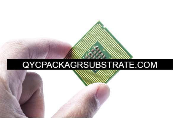
Matriz de cuadrícula de bolas con chip giratorio multichip (FC-BGA) paquete sustratos son componentes integrales en la electrónica avanzada, Proporcionar una plataforma para montar e interconectar múltiples chips semiconductores dentro de un solo paquete.. Estos sustratos están diseñados para admitir aplicaciones informáticas y de comunicación de alto rendimiento., donde una densa integración, transmisión de señal de alta velocidad, y una gestión térmica sólida son esenciales. Este artículo explora las propiedades., estructura, proceso de fabricación, aplicaciones, y ventajas de los sustratos del paquete Multi-Chip FC-BGA.
¿Qué es un sustrato de paquete FC-BGA multichip??
Una matriz de cuadrícula de bolas Flip Chip de múltiples chips (FC-BGA) El sustrato del paquete es una sofisticada placa de circuito impreso. (tarjeta de circuito impreso) que sirve como base para montar múltiples chips semiconductores utilizando tecnología flip-chip. El enfoque del flip-chip implica colocar matrices semiconductoras boca abajo sobre el sustrato., permitiendo conexiones eléctricas directas a través de soldaduras. Este método reduce la longitud de la ruta de la señal., mejora el rendimiento eléctrico, y mejora la disipación del calor.
El sustrato FC-BGA incorpora una matriz de rejilla de bolas. (BGA) de bolas de soldadura en su parte inferior, que facilita el montaje superficial en una placa de circuito impreso (tarjeta de circuito impreso). Esta configuración permite interconexiones de alta densidad., lo que lo hace adecuado para aplicaciones que requieren una potencia computacional sustancial y una transmisión de datos de alta velocidad.
Estructura de los sustratos del paquete Multi-Chip FC-BGA
La estructura de los sustratos del paquete Multi-Chip FC-BGA es compleja y de múltiples capas., Diseñado para adaptarse a los complejos requisitos de las aplicaciones electrónicas de alto rendimiento.. Los elementos estructurales clave incluyen:
La capa central proporciona estabilidad mecánica y forma la base estructural primaria del sustrato.. Por lo general, está hecho de materiales como resina epoxi reforzada con fibra de vidrio o cerámica de alto rendimiento., asegurando robustez y estabilidad dimensional.
Se trata de capas adicionales que se añaden encima de la capa central para aumentar la densidad del cableado y permitir un enrutamiento complejo.. Están construidos con materiales con alto rendimiento térmico y eléctrico para admitir la transmisión de señales y la distribución de energía a alta velocidad..
La máscara de soldadura es una capa protectora que cubre la superficie del sustrato., evitando puentes de soldadura y protegiendo los circuitos subyacentes. Acabados superficiales, como el oro de inmersión de níquel no electrolítico (Aceptar) o conservante orgánico de soldabilidad (OSP), Se aplican a las almohadillas de contacto para garantizar conexiones de soldadura confiables..
Estos incluyen vías, microvías, y orificios pasantes que proporcionan conexiones eléctricas entre diferentes capas del sustrato. Se utilizan técnicas avanzadas como perforación láser y laminación secuencial para crear estas estructuras con alta precisión..
Algunos sustratos FC-BGA multichip incorporan componentes pasivos integrados, como resistencias y condensadores, dentro de las capas del sustrato. Esta integración ayuda a reducir el tamaño total del paquete y mejora el rendimiento eléctrico al minimizar los efectos parásitos..
Materiales utilizados en sustratos de paquete Multi-Chip FC-BGA
Los materiales utilizados en la construcción de los sustratos del paquete Multi-Chip FC-BGA se seleccionan por su excelente rendimiento térmico., eléctrico, y propiedades mecánicas. Los materiales clave incluyen:
Resinas epoxi de alto rendimiento., a menudo reforzado con fibra de vidrio, Se utilizan para las capas centrales y de construcción.. Estos materiales proporcionan la resistencia mecánica y la estabilidad térmica necesarias para un funcionamiento fiable..
El cobre se utiliza ampliamente para las capas conductoras y las interconexiones debido a su excelente conductividad eléctrica.. Se laminan finas láminas de cobre sobre las capas del sustrato y se modelan para formar las trazas del circuito..
Materiales dieléctricos, como poliimida o polímero cristalino líquido (LCP), Se utilizan como capas aislantes entre las pistas conductoras.. Estos materiales tienen constantes dieléctricas y tangentes de pérdida bajas., asegurando una atenuación mínima de la señal y un rendimiento de alta velocidad.
Para mejorar la gestión térmica, materiales de interfaz térmica avanzados (TIM) son usados. Estos materiales facilitan la transferencia eficiente de calor desde las matrices semiconductoras al sustrato., evitando el sobrecalentamiento y garantizando un funcionamiento fiable.
Se aplican acabados superficiales como ENIG u OSP a las almohadillas de contacto para mejorar la soldabilidad y proteger contra la oxidación.. Estos acabados garantizan uniones de soldadura confiables y una durabilidad a largo plazo del sustrato..
El proceso de fabricación de sustratos en paquetes FC-BGA multichip
El proceso de fabricación de sustratos de paquete Multi-Chip FC-BGA implica varios pasos críticos, Cada uno de ellos es esencial para lograr la alta precisión y el rendimiento necesarios para las aplicaciones electrónicas avanzadas.. El proceso incluye:
Materias primas de alta calidad, incluyendo resinas epoxi, láminas de cobre, y películas dieléctricas, están preparados e inspeccionados para garantizar que cumplen con las especificaciones requeridas.
La capa central y las capas de construcción se laminan juntas usando calor y presión para formar un sustrato unificado.. Este paso implica una alineación y un control precisos para garantizar que las capas estén unidas y registradas correctamente..
Se perforan vías y orificios pasantes en el sustrato para crear interconexiones eléctricas entre las capas.. Luego, estos orificios se recubren con cobre para establecer vías conductoras..
Los patrones del circuito se crean mediante procesos fotolitográficos.. Se trata de aplicar una película fotosensible. (fotorresistente) a la superficie de cobre, exponerlo a los rayos ultravioleta (ultravioleta) luz a través de una máscara, y desarrollar las áreas expuestas para revelar los patrones de circuito deseados.. Luego se graba el sustrato para eliminar el cobre no deseado., dejando atrás las huellas del circuito.
Se aplica una máscara de soldadura al sustrato para proteger los circuitos y evitar puentes de soldadura durante el montaje.. La máscara de soldadura generalmente se aplica mediante técnicas de serigrafía o de imágenes fotográficas y luego se cura para endurecerla..
Se aplican acabados superficiales a las almohadillas de contacto para mejorar la soldabilidad y proteger contra la oxidación.. Se utilizan técnicas como ENIG u OSP para garantizar uniones de soldadura confiables y durabilidad a largo plazo..
Los sustratos finales se someten a rigurosas inspecciones y pruebas para garantizar que cumplan con todos los estándares de rendimiento y confiabilidad.. Pruebas electricas, inspección visual, e inspección óptica automatizada (AOI) Se utilizan para identificar cualquier defecto o irregularidad..
Áreas de aplicación de sustratos de paquete Multi-Chip FC-BGA
Los sustratos de paquete Multi-Chip FC-BGA se utilizan en una amplia gama de aplicaciones en diversas industrias debido a sus capacidades de alto rendimiento.. Las áreas de aplicación clave incluyen:
Estos sustratos se utilizan en sistemas informáticos de alto rendimiento., como servidores y centros de datos, donde la integración densa y la transmisión de señales de alta velocidad son esenciales. Admiten procesadores multinúcleo y módulos de memoria avanzados., permitiendo un procesamiento y almacenamiento de datos eficiente.
en telecomunicaciones, Los sustratos Multi-Chip FC-BGA se utilizan en equipos de infraestructura de red, como enrutadores, interruptores, y estaciones base. Sus interconexiones de alta densidad y sus sólidas capacidades de gestión térmica garantizan un rendimiento confiable en entornos de comunicación exigentes..
Los sustratos Multi-Chip FC-BGA se encuentran en la electrónica de consumo, incluyendo teléfonos inteligentes, tabletas, y consolas de juegos. Estos sustratos permiten la integración de múltiples chips semiconductores., proporcionando funcionalidad y rendimiento mejorados en factores de forma compactos.
La industria automotriz utiliza sustratos Multi-Chip FC-BGA en sistemas avanzados de asistencia al conductor (ADA), sistemas de infoentretenimiento, y unidades de control del motor (CUBRIR). Estos sustratos proporcionan el rendimiento y la confiabilidad necesarios para aplicaciones automotrices críticas..
En el sector aeroespacial y de defensa, Los sustratos Multi-Chip FC-BGA se utilizan en aviónica, sistemas de radar, y equipos de comunicación por satélite. Su capacidad para soportar condiciones ambientales adversas y proporcionar transmisión de datos de alta velocidad los hace ideales para estas aplicaciones..
Ventajas de los sustratos del paquete Multi-Chip FC-BGA
Los sustratos de paquete Multi-Chip FC-BGA ofrecen varias ventajas que los convierten en la opción preferida para aplicaciones electrónicas de alto rendimiento.. Estas ventajas incluyen:
Los sustratos Multi-Chip FC-BGA permiten la integración de múltiples chips semiconductores dentro de un solo paquete, Reducir el tamaño y el peso total de los dispositivos electrónicos.. Esta integración de alta densidad es esencial para aplicaciones compactas y portátiles..
La tecnología flip-chip y las estructuras de interconexión avanzadas utilizadas en los sustratos Multi-Chip FC-BGA garantizan una mínima pérdida de señal e interferencias.. Esto da como resultado un rendimiento eléctrico superior y una transmisión de datos de alta velocidad., Crítico para los sistemas electrónicos modernos..
Los sustratos Multi-Chip FC-BGA están diseñados para disipar el calor de manera efectiva, prevenir el sobrecalentamiento y garantizar un funcionamiento confiable de los componentes electrónicos. Los materiales de interfaz térmica avanzados y los diseños térmicos optimizados mejoran la capacidad del sustrato para gestionar el calor..
La construcción robusta y los materiales de alta calidad utilizados en los sustratos Multi-Chip FC-BGA garantizan un rendimiento confiable en entornos exigentes.. Estos sustratos están diseñados para resistir ciclos térmicos., estrés mecánico, y duras condiciones, haciéndolos adecuados para aplicaciones críticas.
Preguntas frecuentes
¿Qué hace que los sustratos de paquete Multi-Chip FC-BGA sean adecuados para aplicaciones electrónicas de alto rendimiento??
Los sustratos de paquete Multi-Chip FC-BGA son ideales para aplicaciones electrónicas de alto rendimiento debido a su integración de alta densidad., rendimiento eléctrico mejorado, gestión térmica eficiente, y propiedades mecánicas robustas. Estas características permiten un funcionamiento fiable y eficiente en entornos exigentes..
¿Se pueden utilizar los sustratos del paquete Multi-Chip FC-BGA en entornos de alta temperatura??
Sí, Los sustratos del paquete Multi-Chip FC-BGA son muy adecuados para entornos de alta temperatura. Sus excelentes capacidades de gestión térmica y su construcción robusta garantizan un rendimiento confiable bajo estrés térmico., haciéndolos ideales para aplicaciones como electrónica automotriz y sistemas aeroespaciales.
¿Cómo garantizan los sustratos del paquete Multi-Chip FC-BGA una gestión térmica eficaz??
Los sustratos del paquete Multi-Chip FC-BGA garantizan una gestión térmica eficaz a través de materiales de interfaz térmica avanzados y diseños térmicos optimizados.. Estas características facilitan la disipación eficiente del calor desde los chips semiconductores al sustrato., evitando el sobrecalentamiento y garantizando un funcionamiento fiable.
¿Qué industrias se benefician más del uso de sustratos de paquete Multi-Chip FC-BGA??
Las industrias que más se benefician del uso de sustratos de paquete Multi-Chip FC-BGA incluyen la informática de alto rendimiento., telecomunicaciones, electrónica de consumo, electrónica automotriz, y aeroespacial y defensa. Estas industrias requieren una integración de alta densidad, rendimiento eléctrico mejorado, y gestión térmica eficiente, qué sustratos Multi-Chip FC-BGA proporcionan.