CO.,LTD")
Hersteller von Multilayer-Last-Leiterplatten. Als führender Hersteller von Multilayer-Last-Leiterplatten, Wir sind auf die Herstellung hochwertiger Produkte spezialisiert, Mehrschichtige Leiterplatten, die den Anforderungen moderner Elektronik gerecht werden. Unsere Leiterplatten sind für den Umgang mit komplexen elektrischen Lasten ausgelegt, Gewährleistung überragender Leistung und Zuverlässigkeit in verschiedenen Anwendungen, von der Telekommunikation bis zur Luft- und Raumfahrt. Mit modernsten Herstellungsverfahren und strenger Qualitätskontrolle, Wir liefern Produkte, die den höchsten Industriestandards entsprechen, Wir bieten maßgeschneiderte Lösungen, die auf unsere Kunden zugeschnitten sind’ spezifische Anforderungen.
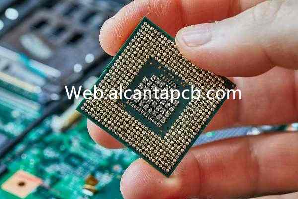
Multilayer-Lastplatinen sind ein Eckpfeiler in der Entwicklung moderner Elektronik, insbesondere in Systemen, die komplexe Schaltkreise erfordern, hohe Zuverlässigkeit, und robuste Leistung. Diese Leiterplatten, mit mehreren Schichten von Leiterbahnen, die durch Isoliermaterialien getrennt sind, sind für anspruchsvolle elektrische Lasten ausgelegt, Damit sind sie im Hochleistungsrechnen unverzichtbar, Telekommunikation, und industrielle Anwendungen. Da sich elektronische Geräte ständig weiterentwickeln, das Bedürfnis nach Effizienz, zuverlässig, und Leiterplatten mit hoher Kapazität werden immer wichtiger, treibt Innovationen in der Multilayer-Last-PCB-Technologie voran.
Was ist eine Multilayer-Lastplatine??
Eine mehrschichtige Ladung Leiterplatte ist eine Leiterplatte, die aus drei oder mehr leitfähigen Schichten besteht, typischerweise aus Kupfer, durch Isolierschichten getrennt. Diese Platinen sind für die Bewältigung höherer elektrischer Lasten und komplexerer Schaltkreise als ein- oder zweilagige Leiterplatten ausgelegt. Die zusätzlichen Schichten ermöglichen komplexere Designs, höhere Bauteildichte, und verbesserte elektrische Leistung, Dadurch eignen sie sich für anspruchsvolle elektronische Anwendungen.
Der Hauptvorteil mehrschichtiger Lastleiterplatten liegt in ihrer Fähigkeit, komplexe elektrische Verbindungen auf kompaktem Raum zu unterstützen. Dies wird durch die Stapelung mehrerer Schichten leitfähiger Bahnen erreicht, die über Vias miteinander verbunden sind – kleine Löcher, die mit leitfähigem Material gefüllt sind. Die Verwendung mehrerer Schichten erhöht nicht nur die Fähigkeit der Leiterplatte, elektrische Signale zu verarbeiten, sondern verbessert auch die Gesamtintegrität und Zuverlässigkeit der Schaltkreise.
Eigenschaften von Multilayer-Last-Leiterplatten
Mehrschichtige Lastleiterplatten zeichnen sich durch mehrere Eigenschaften aus, die sie für Hochleistungsanwendungen geeignet machen:
Die Möglichkeit, mehrere Schichten zu stapeln, ermöglicht die Integration einer größeren Anzahl von Schaltkreisen auf einer einzigen Platine. Dies ist insbesondere bei Anwendungen mit begrenztem Platzangebot von Vorteil, Es ist jedoch eine hohe Funktionalität erforderlich.
Mit mehreren Schichten, Designer können der Stromversorgung bestimmte Ebenen zuweisen, Boden, und Signalrouting, wodurch elektromagnetische Störungen reduziert werden (EMI) und Übersprechen zwischen Signalen. Dadurch wird sichergestellt, dass die Signale sauber und unverzerrt bleiben, auch in komplexen Schaltungen.
Mehrschichtige Lastplatinen ermöglichen eine effizientere Stromverteilung auf der gesamten Platine. Durch die Verwendung dedizierter Strom- und Masseebenen, Die Leiterplatte kann höhere Ströme verarbeiten und die Leistung gleichmäßiger verteilen, Reduziert das Risiko von Hotspots und sorgt für einen stabilen Betrieb.
Durch die Kombination mehrerer Schaltkreise in einer einzigen mehrschichtigen Leiterplatte, die Gesamtgröße und das Gewicht des elektronischen Geräts können reduziert werden. Dies ist besonders wichtig bei Anwendungen wie mobilen Geräten, Luft- und Raumfahrt, und Automobilelektronik, wo Platz und Gewicht entscheidende Faktoren sind.
Mehrschichtige Lastleiterplatten sind auf hohe Zuverlässigkeit ausgelegt, Die zusätzlichen Schichten sorgen für Redundanz und verringern das Ausfallrisiko. Der Einsatz fortschrittlicher Materialien und Herstellungsverfahren verbessert die Haltbarkeit und Leistung dieser Boards in anspruchsvollen Umgebungen zusätzlich.
Herstellungsprozess von Multilayer-Last-Leiterplatten
Die Herstellung mehrschichtiger Lastleiterplatten ist ein komplexer Prozess, der mehrere Schritte umfasst, Jeder Aspekt ist entscheidend für die Leistung und Zuverlässigkeit des Boards:
Der Prozess beginnt mit dem Entwurf des PCB-Layouts mithilfe spezieller Software. Dazu gehört die Erstellung eines detaillierten Streckenplans, einschließlich der Platzierung von Komponenten, Routing von Spuren, und die Anordnung der Schichten. Beim Design müssen Faktoren wie die Signalintegrität berücksichtigt werden, Stromverteilung, und Wärmemanagement.
Bei der Herstellung von mehrschichtigen Lastleiterplatten ist die Materialauswahl von entscheidender Bedeutung. Für die leitfähigen Schichten wird typischerweise hochwertiges Kupfer verwendet, während die Isolierschichten aus Materialien wie FR4 bestehen, Polyimid, oder andere Hochleistungssubstrate. Die Materialien müssen entsprechend den spezifischen Anforderungen der Anwendung ausgewählt werden, einschließlich thermischer Leistung, mechanische Festigkeit, und elektrische Eigenschaften.
Sobald die Materialien ausgewählt sind, Die einzelnen Schichten werden gefertigt. Die Leitermuster werden auf die Kupferschichten geätzt, und die Isolierschichten werden aufgetragen. Diese Schichten werden dann in der richtigen Reihenfolge gestapelt, mit der notwendigen Ausrichtung, um sicherzustellen, dass die Durchkontaktierungen und Durchgangslöcher die Schichten ordnungsgemäß verbinden.
Die gestapelten Schichten werden einem Laminierungsprozess unterzogen, Dort werden sie unter hohem Druck und hoher Temperatur zusammengepresst. Dadurch werden die Schichten zu einer einzigen verbunden, solide Leiterplatte. Der Laminierungsprozess muss sorgfältig kontrolliert werden, um Fehler wie Delamination zu verhindern, verziehen, oder Fehlausrichtung.
Nach dem Laminieren, Löcher werden durch die Leiterplatte gebohrt, um Durchkontaktierungen und Durchgangslöcher zu erzeugen. Diese Löcher werden dann mit einem leitfähigen Material plattiert, typischerweise Kupfer, um die notwendigen elektrischen Verbindungen zwischen den Schichten herzustellen.
Anschließend wird die Leiterplatte einer Oberflächenveredelung unterzogen, Dazu kann auch das Auftragen einer Lötstoppmaske gehören, Siebdruck, und die Abscheidung von Oberflächenveredelungen wie HASL (Heißluft-Lotnivellierung), ZUSTIMMEN (Chemisches Nickel-Immersionsgold), oder andere Beschichtungen, die die Lötbarkeit verbessern und das Kupfer vor Oxidation schützen.
Die fertige Leiterplatte wird strengen Tests unterzogen, um sicherzustellen, dass sie den erforderlichen Spezifikationen entspricht. Dazu gehört auch die elektrische Prüfung zur Prüfung des Durchgangs, Kurzstrecken, und Impedanz, sowie Sichtprüfungen und Zuverlässigkeitstests zur Beurteilung der mechanischen und thermischen Leistung.
Anwendungen von Multilayer-Last-Leiterplatten
Mehrschichtige Lastleiterplatten werden in einem breiten Anwendungsspektrum eingesetzt, vor allem bei hoher Leistung, Zuverlässigkeit, und kompakte Größe sind erforderlich:
In Hochleistungsrechnersystemen, wie Server und Workstations, Mehrschichtige Lastplatinen sind für die Verwaltung der komplexen Schaltkreise und hohen elektrischen Lasten moderner Prozessoren unerlässlich, Speichermodule, und andere kritische Komponenten.
Mehrschichtige Lastleiterplatten werden häufig in Telekommunikationsgeräten verwendet, einschließlich Basisstationen, Router, und Schalter. Diese Leiterplatten unterstützen die Hochgeschwindigkeits-Datenübertragung und komplexe Signalverarbeitung, die für moderne Kommunikationsnetzwerke erforderlich sind.
In der Automobilelektronik, Mehrschichtige Lastleiterplatten werden in fortschrittlichen Fahrerassistenzsystemen eingesetzt (Adas), Motorsteuergeräte (ABDECKUNG), und Infotainmentsysteme. Diese Leiterplatten bieten die Zuverlässigkeit und Leistung, die für den Betrieb in der rauen Automobilumgebung erforderlich sind, wo hohe Temperaturen, Vibrationen, und elektrisches Rauschen sind häufig.
Mehrschichtige Lastleiterplatten werden in industriellen Steuerungssystemen verwendet, Dort verwalten sie die komplexen Schaltkreise, die für die Automatisierung erforderlich sind, Robotik, und Prozesskontrolle. Diese Leiterplatten müssen zuverlässig und langlebig sein, um den anspruchsvollen Bedingungen industrieller Umgebungen standzuhalten.
Vorteile von Multilayer-Last-Leiterplatten
Mehrschichtige Lastleiterplatten bieten mehrere entscheidende Vorteile, die sie für anspruchsvolle elektronische Anwendungen geeignet machen:
Die Möglichkeit, mehrere Schaltkreise auf einer einzigen Platine zu integrieren, reduziert die Gesamtgröße und das Gewicht des elektronischen Geräts, wodurch es kompakter und tragbarer wird.
Mehrschichtige Lastleiterplatten bieten eine verbesserte elektrische Leistung, einschließlich einer besseren Signalintegrität, Stromverteilung, und Wärmemanagement. Dies macht sie ideal für Hochleistungsanwendungen, bei denen Zuverlässigkeit und Effizienz von entscheidender Bedeutung sind.
Mehrschichtige Lastleiterplatten sind auf hohe Zuverlässigkeit ausgelegt, mit zusätzlichen Schichten, die für Redundanz sorgen und das Ausfallrisiko verringern. Dies gewährleistet einen langfristigen Betrieb und reduziert die Wartungskosten.
Die Verwendung mehrerer Schichten ermöglicht eine größere Flexibilität beim PCB-Design, Dies ermöglicht komplexere Schaltkreise und die Integration zusätzlicher Funktionen wie Abschirmung, Erdung, und Stromverteilung.
FAQ
Was sind die Hauptvorteile der Verwendung einer mehrschichtigen Lastplatine??
Mehrschichtige Lastleiterplatten bieten eine erhöhte Schaltungsdichte, Verbesserte Signalintegrität, verbesserte Stromverteilung, reduzierte Größe und Gewicht, und höhere Zuverlässigkeit, Damit sind sie ideal für Hochleistungsanwendungen.
In welchen Branchen werden häufig mehrschichtige Leiterplatten verwendet??
Mehrschichtige Lastleiterplatten werden häufig in Branchen wie dem Hochleistungsrechnen eingesetzt, Telekommunikation, Automobilelektronik, und industrielle Kontrollsysteme, wo sie komplexe Schaltkreise und hohe elektrische Lasten bewältigen.
Wie werden mehrschichtige Lastleiterplatten hergestellt??
Der Herstellungsprozess umfasst Design und Layout, Materialauswahl, Schichtstapelung, Laminierung, Bohren und Beschichten, Oberflächenveredelung, und strenge Tests, um Leistung und Zuverlässigkeit sicherzustellen.
Warum ist die Signalintegrität bei mehrschichtigen Lastleiterplatten wichtig??
Die Signalintegrität ist bei mehrschichtigen Lastleiterplatten von entscheidender Bedeutung, um sicherzustellen, dass elektrische Signale sauber und unverzerrt bleiben, Reduzierung des Risikos elektromagnetischer Störungen und Übersprechen zwischen Signalen.