CO.,LTD")
Hersteller von FPGA-Gehäusesubstraten. Ein Hersteller von FPGA-Gehäusesubstraten ist auf die Entwicklung und Produktion fortschrittlicher Substrate für feldprogrammierbare Gate-Arrays spezialisiert (FPGAs). Diese Substrate gewährleisten eine optimale Leistung, Signalintegrität, und Wärmemanagement für FPGAs, die im Hochleistungsrechnen von entscheidender Bedeutung sind, Telekommunikation, und verschiedene industrielle Anwendungen. Einsatz modernster Materialien und Fertigungstechniken, Der Hersteller liefert zuverlässig, hochdichte Substrate, die den hohen Anforderungen moderner Elektronik gerecht werden, Dies ermöglicht schnellere und effizientere FPGA-Lösungen für eine Vielzahl von Branchen.
FPGA (Feldprogrammierbares Gate-Array) Verpackungssubstrate spielen in der modernen Elektronik eine entscheidende Rolle, insbesondere bei Hochleistungsanwendungen, bei denen eine individuelle Anpassung erforderlich ist, Flexibilität, und Geschwindigkeit stehen im Vordergrund. Diese Substrate bilden die physikalische und elektrische Grundlage für FPGAs, Dabei handelt es sich um Halbleiterbauelemente, die vom Benutzer nach der Herstellung konfiguriert werden können. Da die Nachfrage nach fortschrittlicherer und effizienterer Elektronik wächst, FPGA-Gehäusesubstrate sind zu unverzichtbaren Komponenten in Branchen wie der Telekommunikation geworden, Luft- und Raumfahrt, Automobil, und Unterhaltungselektronik.
Was sind FPGA-Paketsubstrate??
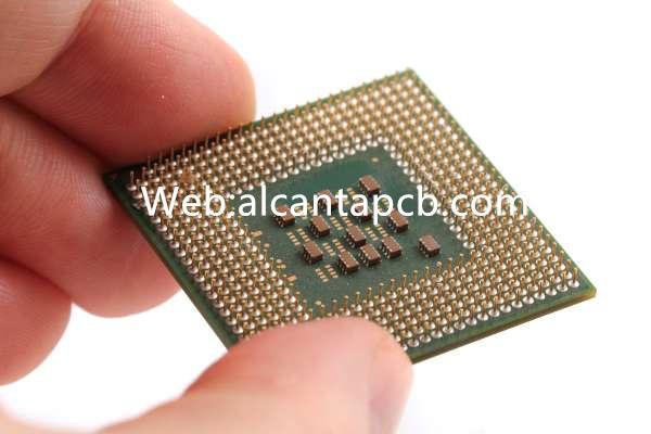
FPGA-Gehäusesubstrate sind mehrschichtige Strukturen, die den FPGA-Chip tragen und mit der Leiterplatte verbinden (Leiterplatte). Diese Substrate sind dafür verantwortlich, die elektrischen Verbindungen zwischen dem FPGA und dem Rest des Systems sicherzustellen, sowie mechanische Unterstützung und Wärmemanagement. Das Design und die Materialauswahl der FPGA-Gehäusesubstrate sind entscheidend, da sie sich direkt auf die Leistung auswirken, Zuverlässigkeit, und Langlebigkeit des FPGA.
FPGA-Gehäusesubstrate bestehen typischerweise aus mehreren Schichten leitender und isolierender Materialien, wie Kupfer und Epoxidharz, in einer bestimmten Konfiguration angeordnet, um die elektrische Leistung zu optimieren. Diese Schichten sind durch Vias miteinander verbunden, Dabei handelt es sich um kleine Löcher, die mit leitfähigem Material gefüllt sind und die Signalübertragung zwischen den Schichten ermöglichen. Die Komplexität und Präzision des Substratdesigns sind für die Aufrechterhaltung der Integrität der vom FPGA verarbeiteten Hochgeschwindigkeitssignale von entscheidender Bedeutung.
Eigenschaften von FPGA-Paketsubstraten
Mehrere Schlüsselmerkmale definieren FPGA-Gehäusesubstrate und machen sie für den Einsatz in Hochleistungsanwendungen geeignet:
FPGA-Gehäusesubstrate nutzen häufig die HDI-Technologie, Dies ermöglicht eine größere Anzahl von Verbindungen auf kleinerem Raum. Dies wird durch die Verwendung feinerer Linien erreicht, kleinere Durchkontaktierungen, und dichter gepackte Komponenten, Dadurch kann der FPGA komplexe Vorgänge mit hoher Geschwindigkeit ausführen.
Die Aufrechterhaltung der Signalintegrität ist bei FPGA-Gehäusesubstraten von entscheidender Bedeutung, zumal FPGAs häufig in Anwendungen eingesetzt werden, die eine Hochgeschwindigkeits-Datenverarbeitung erfordern. Das Substrat muss so gestaltet sein, dass der Signalverlust minimiert wird, Übersprechen, und elektromagnetische Störungen (EMI), Sicherstellen, dass das FPGA effizient und genau arbeiten kann.
FPGAs erzeugen im Betrieb erhebliche Wärme, insbesondere bei der Verarbeitung großer Datenmengen oder der Durchführung komplexer Berechnungen. FPGA-Gehäusesubstrate sind so konzipiert, dass sie Wärme effektiv ableiten, Verhindert einen thermischen Aufbau, der das FPGA beschädigen oder seine Leistung beeinträchtigen könnte. Dies wird durch den Einsatz thermischer Vias erreicht, Kühlkörper, und wärmeleitende Materialien innerhalb des Substrats.
FPGA-Gehäusesubstrate müssen äußerst zuverlässig sein, insbesondere in geschäftskritischen Anwendungen wie der Luft- und Raumfahrt oder medizinischen Geräten. Sie sind so konzipiert, dass sie rauen Umgebungsbedingungen standhalten, einschließlich Temperaturschwankungen, mechanische Beanspruchung, und Feuchtigkeitseinwirkung. Der Einsatz hochwertiger Materialien und fortschrittlicher Herstellungsverfahren stellt sicher, dass das Substrat über die gesamte Lebensdauer des FPGA stabil und funktionsfähig bleibt.
Einer der Hauptvorteile von FPGAs ist ihre Fähigkeit, für verschiedene Aufgaben neu programmiert zu werden. FPGA-Gehäusesubstrate sind unter Berücksichtigung dieser Flexibilität konzipiert, Dies ermöglicht die Integration verschiedener Komponenten und Verbindungen, die die spezifischen Anforderungen der Anwendung unterstützen können. Diese Anpassung erstreckt sich auch auf das Substrat selbst, wo die Anzahl der Schichten, Materialarten, und Trace-Konfigurationen können angepasst werden, um die Leistung zu optimieren.
Herstellungsprozess von FPGA-Paketsubstraten
Die Herstellung von FPGA-Gehäusesubstraten ist ein komplexer Prozess, der mehrere kritische Schritte umfasst, Jedes ist darauf ausgelegt, ein Höchstmaß an Leistung und Zuverlässigkeit zu gewährleisten:
Der Prozess beginnt mit der Gestaltung des Substratlayouts mithilfe fortschrittlicher computergestützter Konstruktion (CAD) Werkzeuge. Ingenieure simulieren die elektrische Leistung des Substrats, unter Berücksichtigung von Faktoren wie der Signalintegrität, Wärmemanagement, und mechanische Stabilität. Diese Phase ist entscheidend für die Identifizierung potenzieller Probleme und die Optimierung des Designs, bevor mit der Fertigung begonnen wird.
The choice of materials is essential in determining the performance of the FPGA package substrate. Common materials include copper for conductive layers, und verschiedene Arten von Epoxidharzen, Keramik, oder Polyimide für Isolierschichten. The materials are selected based on their electrical, Thermal-, und mechanische Eigenschaften, as well as their compatibility with the FPGA and the intended application.
Sobald die Materialien ausgewählt sind, the individual layers of the substrate are fabricated. Conductive patterns are etched onto the copper layers, und Isolierschichten werden aufgetragen. These layers are then stacked in a specific order and laminated under high pressure and temperature to form a single, fester Untergrund. The alignment and bonding of the layers are critical to ensuring the proper functioning of the FPGA.
In das Substrat werden Durchkontaktierungen gebohrt, um elektrische Verbindungen zwischen den Schichten herzustellen. Diese Durchkontaktierungen werden dann mit leitfähigem Material plattiert, typischerweise Kupfer, die notwendigen Verbindungen herzustellen. Die Präzision des Via-Bildungsprozesses ist für die Aufrechterhaltung der Signalintegrität und die Gewährleistung, dass das FPGA mit hohen Geschwindigkeiten arbeiten kann, von entscheidender Bedeutung.
Nachdem das Substrat vollständig montiert ist, Es wird einer Oberflächenveredelung unterzogen, um seine Haltbarkeit und Lötbarkeit zu verbessern. Dies kann das Aufbringen von Schutzbeschichtungen umfassen, Lötmaske, und Oberflächenveredelungen wie ENIG (Chemisches Nickel-Immersionsgold). Der letzte Schritt umfasst strenge Tests zur Überprüfung der elektrischen Leistung, Wärmemanagement, und mechanische Integrität des Substrats.
Anwendungen von FPGA-Paketsubstraten
FPGA-Gehäusesubstrate werden in einer Vielzahl von Anwendungen in verschiedenen Branchen eingesetzt, wo ihre Leistung und Zuverlässigkeit von entscheidender Bedeutung sind:
In der Telekommunikation, FPGAs werden zur Signalverarbeitung verwendet, Datenverschlüsselung, und Netzwerkmanagement. FPGA-Gehäusesubstrate in diesem Bereich müssen eine Hochgeschwindigkeits-Datenübertragung unterstützen und die Signalintegrität über große Entfernungen aufrechterhalten.
In der Luft- und Raumfahrt und Verteidigung, FPGAs werden in Radarsystemen eingesetzt, Satellitenkommunikation, und Avionik. Die Substrate müssen äußerst zuverlässig sein und extremen Umweltbedingungen standhalten, einschließlich Temperaturschwankungen, Strahlung, und mechanischer Schock.
In der Automobilindustrie, FPGAs werden in fortschrittlichen Fahrerassistenzsystemen eingesetzt (Adas), Infotainmentsysteme, und Motorsteuergeräte (ABDECKUNG). Die Substrate müssen ein robustes Wärmemanagement und Haltbarkeit bieten, um unter den rauen Bedingungen im Automobilumfeld zu funktionieren.
In der Unterhaltungselektronik, FPGAs werden in Geräten wie Smartphones eingesetzt, Tabletten, und Gaming -Konsolen. Die Untergründe müssen kompakt und leicht sein, mit der Fähigkeit, die für Multimedia-Anwendungen erforderliche Hochgeschwindigkeitsverarbeitung zu unterstützen.
Vorteile von FPGA-Paketsubstraten
FPGA-Gehäusesubstrate bieten mehrere entscheidende Vorteile, die sie in der modernen Elektronik unverzichtbar machen:
FPGA-Gehäusesubstrate können auf die spezifischen Anforderungen der Anwendung zugeschnitten werden, Dies ermöglicht eine größere Flexibilität und Leistungsoptimierung.
Die Substrate sind so konzipiert, dass Signalverluste minimiert werden, Übersprechen, und EMI, Sicherstellen, dass das FPGA effizient und genau arbeitet.
FPGA-Gehäusesubstrate sind mit fortschrittlichen Wärmemanagementfunktionen ausgestattet, die eine Überhitzung verhindern und einen stabilen Betrieb gewährleisten.
Die Substrate sind so konstruiert, dass sie rauen Umgebungsbedingungen standhalten, Dadurch eignen sie sich für den Einsatz in geschäftskritischen Anwendungen.
FAQ
Welche Materialien werden üblicherweise in FPGA-Gehäusesubstraten verwendet??
FPGA-Gehäusesubstrate werden typischerweise aus Materialien wie Kupfer für leitende Schichten und Epoxidharzen hergestellt, Keramik, oder Polyimide für Isolierschichten.
Wie unterstützen FPGA-Gehäusesubstrate die Hochgeschwindigkeitsdatenverarbeitung??
FPGA-Gehäusesubstrate unterstützen die Hochgeschwindigkeitsdatenverarbeitung durch den Einsatz der HDI-Technologie, Minimierung von Signalverlust und Übersprechen, und sorgt für ein effektives Wärmemanagement.
Warum ist das Wärmemanagement bei FPGA-Gehäusesubstraten wichtig??
Das Wärmemanagement ist von entscheidender Bedeutung, da FPGAs während des Betriebs erhebliche Wärme erzeugen, und eine effektive Wärmeableitung verhindert Schäden am FPGA und sorgt für eine gleichbleibende Leistung.
Welche Branchen verwenden üblicherweise FPGA-Gehäusesubstrate??
FPGA-Gehäusesubstrate werden häufig in der Telekommunikation verwendet, Luft- und Raumfahrt und Verteidigung, Automobilelektronik, und Unterhaltungselektronik, wo hohe Leistung und Zuverlässigkeit unerlässlich sind.