CO.,LTD")
Hersteller von Ultra-Multilayer-FCCSP-Substraten. Ein FPGA Paketsubstrate Der Hersteller ist auf die Entwicklung und Herstellung fortschrittlicher Substrate für feldprogrammierbare Gate-Arrays spezialisiert (FPGAs). Diese Substrate gewährleisten eine optimale Leistung, Signalintegrität, und Wärmemanagement für FPGAs, die im Hochleistungsrechnen von entscheidender Bedeutung sind, Telekommunikation, und verschiedene industrielle Anwendungen. Einsatz modernster Materialien und Fertigungstechniken, Der Hersteller liefert zuverlässig, hochdichte Substrate, die den hohen Anforderungen moderner Elektronik gerecht werden, Dies ermöglicht schnellere und effizientere FPGA-Lösungen für eine Vielzahl von Branchen.
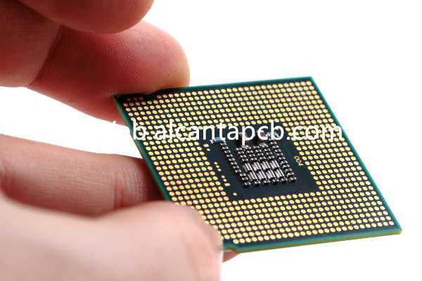
Ultra-mehrschichtiges FCCSP (Flip-Chip-Chip-Waage-Paket) Substrate stellen einen bedeutenden Fortschritt in der Halbleiterverpackungstechnologie dar. Diese Substrate sind so konzipiert, dass sie der zunehmenden Komplexität und Miniaturisierung moderner elektronischer Geräte gerecht werden. Mit dem Aufkommen des Hochleistungsrechnens, Telekommunikation, und Unterhaltungselektronik, das Bedürfnis nach Effizienz, kompakt, und zuverlässige Verpackungslösungen ist gewachsen. Ultra-mehrschichtiges FCCSP Substrate erfüllen diese Anforderungen durch eine verbesserte elektrische Leistung, überlegene Wärmeableitung, und erhöhte Verbindungsdichte.
Was sind Ultra-Multilayer-FCCSP-Substrate??
Ultra-mehrschichtige FCCSP-Substrate sind spezielle Verpackungsplattformen zur Montage und Verbindung von Halbleiterchips, insbesondere in Flip-Chip-Konfigurationen. Im Gegensatz zu herkömmlichen Verpackungsmethoden, wo der Chip mit Drähten verbunden ist, Bei der Flip-Chip-Technologie werden die Bumps oder Pads des Chips direkt mit dem Substrat verbunden, Dies ermöglicht eine höhere Verbindungsdichte und eine bessere elektrische Leistung. Der “Ultra-Multilayer” Der Aspekt bezieht sich auf die mehreren Schichten aus leitenden und isolierenden Materialien des Substrats, die zu einem kompakten und dennoch hochfunktionalen Paket gestapelt werden.
Diese Substrate sind für Anwendungen, die eine Hochgeschwindigkeits-Datenverarbeitung erfordern, unerlässlich, wo die Minimierung der Signalverzögerung und die Maximierung der Signalintegrität entscheidend sind. Die mehreren Schichten in den FCCSP-Substraten stellen die notwendigen Pfade für elektrische Signale bereit und sorgen gleichzeitig dafür, dass das Gehäuse kompakt und effizient bleibt. Zusätzlich, Die Flip-Chip-Konfiguration ermöglicht eine effizientere Wärmeableitung, ein entscheidender Faktor für die Aufrechterhaltung der Leistung und Langlebigkeit von Halbleiterbauelementen.
Eigenschaften von Ultra-Multilayer-FCCSP-Substraten
Mehrere unterschiedliche Eigenschaften zeichnen ultramehrschichtige FCCSP-Substrate aus, Dadurch sind sie für Hochleistungsanwendungen geeignet:
Einer der bedeutendsten Vorteile von Ultra-Multilayer-FCCSP-Substraten ist ihre Fähigkeit, eine hohe Verbindungsdichte zu unterstützen. Dies wird durch die Verwendung von feinen Linienmustern und Mikrovias erreicht, die eine größere Anzahl von Verbindungen auf kleinerem Raum ermöglichen. Diese hohe Dichte ist für Anwendungen, bei denen der Platz knapp ist, von entscheidender Bedeutung, und die Leistung darf nicht beeinträchtigt werden.
Die in FCCSP-Substraten verwendete Flip-Chip-Konfiguration macht lange Drahtbonds überflüssig, Reduzierung der parasitären Induktivität und Kapazität. Dies führt zu einer besseren elektrischen Leistung, mit schnellerer Signalübertragung und reduziertem Signalverlust. Der mehrschichtige Aufbau ermöglicht zudem die Trennung unterschiedlicher Signaltypen, weitere Leistungssteigerung durch Minimierung von Übersprechen und Interferenzen.
Die Wärmeableitung ist ein entscheidender Faktor für die Aufrechterhaltung der Leistung und Zuverlässigkeit von Halbleiterbauelementen. Ultra-mehrschichtige FCCSP-Substrate wurden unter Berücksichtigung des Wärmemanagements entwickelt, Es verfügt über Funktionen wie thermische Durchkontaktierungen und Wärmeverteiler, um die Wärme effizient vom Chip abzuleiten. Dadurch wird sichergestellt, dass das Gerät innerhalb seines optimalen Betriebstemperaturbereichs bleibt, verhindert Überhitzung und verlängert die Lebensdauer.
Da elektronische Geräte immer kleiner werden, Die Nachfrage nach kompakteren Verpackungslösungen ist gestiegen. Ultra-mehrschichtige FCCSP-Substrate erfüllen diese Anforderung, indem sie eine hochintegrierte Lösung bieten, die den gesamten Platzbedarf des Geräts minimiert. Trotz ihrer kompakten Größe, Diese Substrate gehen keine Kompromisse bei der Leistung ein, Damit sind sie ideal für Anwendungen mit begrenztem Platzangebot.
Zusätzlich zu ihren Leistungsmerkmalen, Ultra-Multilayer-FCCSP-Substrate sind auch für ihre Zuverlässigkeit bekannt. Sie sind so konzipiert, dass sie den Belastungen durch Temperaturwechsel standhalten, mechanischer Schock, und andere Umweltfaktoren, die die Leistung des Halbleiterbauelements beeinträchtigen könnten. Diese Zuverlässigkeit ist für Anwendungen in Branchen wie der Automobilindustrie von entscheidender Bedeutung, Luft- und Raumfahrt, und Telekommunikation, wo Scheitern keine Option ist.
Herstellungsprozess von Ultra-Multilayer-FCCSP-Substraten
Der Herstellungsprozess von Ultra-Multilayer-FCCSP-Substraten umfasst mehrere Schlüsselschritte, Jeder Aspekt ist entscheidend für die Gewährleistung der Leistung und Zuverlässigkeit des Endprodukts:
Der Prozess beginnt mit der Gestaltung des Untergrundes, Hier verwenden Ingenieure fortschrittliche CAD-Tools, um das Layout der leitenden und isolierenden Schichten zu erstellen. Diese Entwurfsphase ist entscheidend für die Optimierung der elektrischen Leistung des Substrats, Außerdem muss sichergestellt werden, dass es den spezifischen Anforderungen der Anwendung gerecht wird.
Die Auswahl der Materialien ist ein entscheidender Aspekt des Herstellungsprozesses. Die leitenden Schichten bestehen typischerweise aus hochreinem Kupfer, während die Isolierschichten aus Epoxidharzen bestehen können, Polyimide, oder andere fortschrittliche Materialien. Die Auswahl der Materialien basiert auf Faktoren wie der elektrischen Leitfähigkeit, thermische Leistung, und mechanische Festigkeit.
Sobald die Materialien ausgewählt wurden, Die einzelnen Schichten werden hergestellt und gestapelt, um das Substrat zu bilden. Dieser Stapelvorgang muss mit Präzision durchgeführt werden, um sicherzustellen, dass die Schichten korrekt ausgerichtet sind. Anschließend wird der Stapel unter hohem Druck und hoher Temperatur laminiert, Zusammenfügen der Schichten zu einer einzigen, solide Struktur.
In das Substrat werden Durchkontaktierungen gebohrt, um elektrische Verbindungen zwischen den Schichten herzustellen. Diese Durchkontaktierungen werden dann mit Kupfer oder anderen leitenden Materialien plattiert, um die notwendigen Pfade für elektrische Signale herzustellen. Die Genauigkeit dieses Schritts ist entscheidend für die Aufrechterhaltung der Integrität der Hochgeschwindigkeitssignale, die das Substrat passieren.
Nachdem das Substrat vollständig montiert wurde, Es wird einer Oberflächenveredelung unterzogen, Dazu kann auch die Anwendung einer Lötmaske gehören, Schutzbeschichtungen, und Oberflächenveredelungen wie ENIG (Chemisches Nickel-Immersionsgold). Der letzte Schritt im Herstellungsprozess ist das Testen, Dabei wird das Substrat strengen elektrischen und mechanischen Tests unterzogen, um sicherzustellen, dass es alle Spezifikationen erfüllt.
Anwendungen von Ultra-Multilayer-FCCSP-Substraten
Ultra-mehrschichtige FCCSP-Substrate werden in einer Vielzahl von Anwendungen in verschiedenen Branchen eingesetzt, wo ihre einzigartigen Eigenschaften für die Erzielung hoher Leistungen von entscheidender Bedeutung sind:
In Hochleistungsrechneranwendungen, wie Server und Rechenzentren, Ultra-mehrschichtige FCCSP-Substrate bieten die erforderliche Verbindungsdichte und elektrische Leistung, um die anspruchsvollen Verarbeitungsaufgaben zu unterstützen.
Telekommunikationsausrüstung, wie Netzwerk-Switches und Router, Profitieren Sie von den Hochgeschwindigkeits-Signalübertragungsfähigkeiten von Ultra-Multilayer-FCCSP-Substraten. Diese Substrate gewährleisten zuverlässige Leistung auch in den datenintensivsten Umgebungen.
In der Unterhaltungselektronik, wie Smartphones und Tablets, Das kompakte Design und die Hochleistungseigenschaften von Ultra-Multilayer-FCCSP-Substraten machen sie ideal für die Unterstützung erweiterter Funktionen bei gleichzeitig kleinem Formfaktor.
Die Zuverlässigkeit und die Wärmemanagementfähigkeiten von Ultra-Multilayer-FCCSP-Substraten machen sie gut für die Automobilelektronik geeignet, wo sie in fortschrittlichen Fahrerassistenzsystemen zum Einsatz kommen (Adas), Infotainmentsysteme, und mehr.
Vorteile von Ultra-Multilayer-FCCSP-Substraten
Ultra-mehrschichtige FCCSP-Substrate bieten mehrere entscheidende Vorteile, die sie in der modernen Elektronik unverzichtbar machen:
Die Fähigkeit, eine hohe Verbindungsdichte zu unterstützen, ermöglicht kompaktere und effizientere Designs, insbesondere bei platzbeschränkten Anwendungen.
Der Wegfall von Drahtverbindungen und die Verwendung fortschrittlicher Materialien führen zu einer schnelleren Signalübertragung und einem geringeren Signalverlust, Verbesserung der Gesamtleistung des Geräts.
Die fortschrittlichen Wärmemanagementfunktionen von Ultra-Multilayer-FCCSP-Substraten tragen dazu bei, optimale Betriebstemperaturen aufrechtzuerhalten, verhindert Überhitzung und sorgt für langfristige Zuverlässigkeit.
Die Kombination aus kompaktem Design und robuster Zuverlässigkeit macht ultra-mehrschichtige FCCSP-Substrate ideal für den Einsatz in einer Vielzahl von Anwendungen, von der Unterhaltungselektronik bis hin zu Industriesystemen.
FAQ
Welche Hauptmaterialien werden in Ultra-Multilayer-FCCSP-Substraten verwendet??
Als Materialien kommen vor allem hochreines Kupfer für die Leitschichten und Epoxidharze zum Einsatz, Polyimide, oder andere fortschrittliche Materialien für Isolierschichten.
Warum ist das Wärmemanagement bei ultramehrschichtigen FCCSP-Substraten wichtig??
Ein wirksames Wärmemanagement ist von entscheidender Bedeutung, da es hilft, Überhitzung zu verhindern, Dies kann die Leistung und Lebensdauer des Halbleiterbauelements beeinträchtigen.
In welchen Branchen werden häufig ultramehrschichtige FCCSP-Substrate verwendet??
Diese Substrate werden häufig in Branchen wie dem Hochleistungsrechnen verwendet, Telekommunikation, Unterhaltungselektronik, und Automobilelektronik.
Wie verbessern ultra-mehrschichtige FCCSP-Substrate die Signalintegrität??
Ultra-mehrschichtige FCCSP-Substrate verbessern die Signalintegrität durch Minimierung parasitärer Induktivität und Kapazität, Reduzierung des Signalverlusts, und Trennen verschiedener Signaltypen innerhalb der mehrschichtigen Struktur.