CO., LTD")
Fabricante de PCB de RF. Un fabricante de PCB de RF se especializa en el diseño y producción de placas de circuito impreso para aplicaciones de radiofrecuencia.. Estos PCB Son esenciales para la transmisión de señales de alta frecuencia en dispositivos de comunicación inalámbrica., sistemas de radar, y tecnología satelital. El fabricante garantiza una alta calidad., Fabricación precisa para cumplir con los estrictos requisitos de rendimiento de RF., incluyendo integridad de la señal y mínima interferencia, proporcionando soluciones confiables para electrónica avanzada.
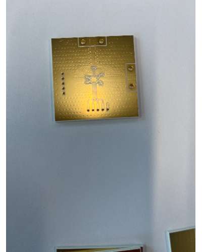
PCB de RF (Placas de circuito impreso de radiofrecuencia) Son placas de circuito especializadas diseñadas para funcionar en radiofrecuencias., normalmente van desde 3 kHz a 300 GHz. Estos PCB son fundamentales en aplicaciones que requieren una transmisión de señal precisa y eficiente con pérdidas y distorsiones mínimas.. Este artículo explora las propiedades., estructura, materiales, procesos de fabricación, aplicaciones, ventajas, y preguntas frecuentes (Preguntas frecuentes) relacionado con PCB de RF.
Estructura de los PCB de RF
La estructura de los PCB de RF está meticulosamente diseñada para soportar alta frecuencia integridad y rendimiento de la señal:
El sustrato suele estar hecho de materiales con una constante dieléctrica y una tangente de pérdida bajas., como PTFE (politetrafluoroetileno), Laminados Rogers, o composites de PTFE rellenos de cerámica. Estos materiales ayudan a minimizar la pérdida de señal y garantizar un rendimiento estable en altas frecuencias..
Para las trazas se utilizan capas finas de cobre u otros metales conductores., asegurando una pérdida mínima de señal y un rendimiento de alta frecuencia. Estas capas suelen estar grabadas con precisión para formar los patrones de circuito necesarios..
Se utilizan materiales dieléctricos de alto rendimiento para separar capas conductoras., Mantener el aislamiento eléctrico y la integridad de la señal.. Estas capas son cruciales para prevenir interferencias de señales y diafonía entre trazas adyacentes..
Los planos de tierra dedicados proporcionan un plano de referencia para las señales., reducir la interferencia electromagnética (EMI) y mejorar la calidad de la señal. Los planos de tierra también desempeñan un papel vital en la gestión térmica al disipar el calor generado por operaciones de alta frecuencia..
Las interconexiones verticales conectan diferentes capas de la PCB, permitiendo enrutamiento complejo y diseños de alta densidad. Microvías, En particular, Se utilizan en interconexión de alta densidad. (IDH) diseños para minimizar la inductancia y capacitancia parásitas.
Recubrimientos protectores como ENIG (Oro de inmersión de níquel electroutolante) o OSP (Conservantes de soldabilidad orgánicos) Se utilizan para mejorar la soldabilidad y proteger contra la oxidación.. Estos acabados también ayudan a garantizar conexiones eléctricas confiables..
Materiales utilizados en PCB de RF
Los materiales clave utilizados en los PCB de RF incluyen:
Un material dieléctrico de bajas pérdidas conocido por su excelente rendimiento y estabilidad en alta frecuencia.. El PTFE se utiliza a menudo en aplicaciones que requieren una atenuación mínima de la señal y una alta integridad de la señal..
Laminados de alto rendimiento con baja constante dieléctrica y tangente de pérdida, Diseñado específicamente para aplicaciones de RF y microondas.. Los materiales Rogers son los preferidos por sus propiedades eléctricas consistentes y su confiabilidad en altas frecuencias..
Estos materiales ofrecen un equilibrio de bajas pérdidas., alta conductividad térmica, y estabilidad mecánica. A menudo se utilizan en aplicaciones donde la gestión térmica y la robustez mecánica son fundamentales..
El cobre de alta pureza se utiliza para trazas conductoras debido a su excelente conductividad eléctrica y confiabilidad.. La baja resistencia del cobre ayuda a mantener la integridad de la señal en altas frecuencias.
Materiales con baja constante dieléctrica y tangente de pérdida., como el teflón (PTFE) y materiales Rogers especializados, Se utilizan para garantizar una mínima pérdida de señal y distorsión.. Estos materiales son cruciales para mantener una alta calidad de señal..
Proceso de fabricación de PCB de RF
El proceso de fabricación de PCB de RF implica varios pasos precisos para garantizar el rendimiento y la confiabilidad de alta frecuencia.:
Elegir materiales base y capas conductoras adecuadas en función de los requisitos de rendimiento. El proceso de selección considera factores como la constante dieléctrica., pérdida tangente, propiedades térmicas, y resistencia mecánica.
Apilar y unir múltiples capas de materiales conductores y dieléctricos en condiciones controladas para formar una PCB estable. Este proceso garantiza una alineación y un espesor de capa consistentes..
Perforación de precisión para crear vías y microvías para interconexiones verticales entre capas.. A menudo se utilizan técnicas avanzadas de perforación láser para microvías para lograr una alta precisión y un daño mínimo a los materiales circundantes..
Galvanoplastia de cobre sobre el sustrato y las vías internas para establecer conexiones eléctricas confiables.. Este paso garantiza vías fuertes y conductoras para la transmisión de señales..
Uso de fotolitografía y grabado químico para definir los patrones de circuitos y las interconexiones.. Un patrón preciso es esencial para lograr el diseño y el rendimiento del circuito deseados..
Aplicar revestimientos protectores a superficies de cobre expuestas para mejorar la soldabilidad y proteger contra la oxidación.. Los acabados superficiales también ayudan a prevenir la corrosión y garantizar la confiabilidad a largo plazo..
Fijación de componentes mediante técnicas de soldadura adecuadas para aplicaciones de alta frecuencia, asegurando una mínima pérdida de señal y distorsión. El proceso de ensamblaje incluye la colocación y soldadura cuidadosa de los componentes de RF para mantener la integridad de la señal..
Pruebas rigurosas de rendimiento eléctrico, integridad de la señal, y cumplimiento de las especificaciones de diseño.. Las pruebas incluyen mediciones de pérdida de señal., comprobaciones de impedancia, y ciclos térmicos para garantizar la confiabilidad en condiciones de operación.
Aplicaciones de PCB de RF
Los PCB de RF se utilizan en una amplia gama de aplicaciones de alta frecuencia, incluido:
Estaciones base, antenas, y módulos RF para redes de comunicación móviles e inalámbricas. Los PCB de RF son esenciales para transmitir y recibir señales de alta frecuencia en sistemas de comunicación.
Sistemas de radar de alta frecuencia utilizados en defensa., aeroespacial, y aplicaciones automotrices. Los PCB de RF permiten el procesamiento y la transmisión precisos de señales en sistemas de radar.
Equipos de diagnóstico e imagen., como máquinas de resonancia magnética y ultrasonido, que requieren procesamiento de señales de alta frecuencia. Los PCB RF garantizan una transmisión de señales precisa y confiable en dispositivos médicos.
Transpondedores, receptores, y transmisores utilizados en sistemas de comunicación por satélite. Los PCB de RF admiten enlaces de comunicación de alta frecuencia en sistemas satelitales.
Sensores y sistemas de control de alta frecuencia utilizados en entornos de control de procesos y fabricación.. Los PCB RF permiten un procesamiento de señales confiable y eficiente en la automatización industrial.
Ventajas de los PCB de RF
Los PCB de RF ofrecen varias ventajas importantes:
Diseñado para soportar frecuencias de RF con mínima pérdida de señal y distorsión.. Los PCB RF garantizan una alta integridad de la señal y rendimiento a altas frecuencias.
Mantiene la calidad e integridad de la señal mediante el uso de materiales de baja pérdida y procesos de fabricación precisos.. Los PCB de RF minimizan la atenuación y la interferencia de la señal.
La construcción y las pruebas robustas garantizan el rendimiento y la confiabilidad a largo plazo en aplicaciones exigentes de alta frecuencia.. Los PCB RF están diseñados para soportar duras condiciones de funcionamiento.
Disipación de calor efectiva a través de materiales del sustrato y características de diseño., asegurando un funcionamiento estable en condiciones de alta potencia. Los PCB de RF evitan el sobrecalentamiento y el daño térmico.
Adecuado para una amplia gama de aplicaciones de alta frecuencia en diversas industrias. Los PCB de RF se pueden personalizar para cumplir con requisitos específicos de diseño y rendimiento..
Preguntas frecuentes
¿Qué materiales se utilizan normalmente para los PCB de RF?, y por qué?
Los PCB de RF suelen utilizar materiales como PTFE, Laminados Rogers, y compuestos de PTFE rellenos de cerámica por su baja constante dieléctrica, tangente de baja pérdida, y estabilidad de alta frecuencia. Estos materiales son esenciales para mantener la integridad y el rendimiento de la señal..
¿En qué se diferencian los PCB RF de los PCB estándar??
Los PCB RF están diseñados específicamente para aplicaciones de alta frecuencia, utilizando materiales y procesos de fabricación especializados para minimizar la pérdida y distorsión de la señal. Los PCB estándar se utilizan normalmente para aplicaciones de baja frecuencia y es posible que no requieran características de rendimiento tan estrictas..
¿Qué industrias se benefician más del uso de PCB de RF??
Industrias como las telecomunicaciones., aeroespacial y defensa, dispositivos médicos, Comunicaciones por satélite, y la automatización industrial se benefician significativamente del uso de PCB de RF debido a su rendimiento y confiabilidad de alta frecuencia..
¿Cómo se prueban los PCB de RF para garantizar la confiabilidad??
Los PCB de RF se someten a rigurosos procesos de prueba, incluidas pruebas eléctricas para la integridad y el rendimiento de la señal, ciclo térmico, y pruebas de confiabilidad. Estas pruebas garantizan que los PCB de RF cumplan con estrictos estándares de durabilidad y rendimiento de alta frecuencia..