CO., LTD")
Semiconductor sustrato BGAFabricante, Producimos principalmente sustratos de paso ultrapequeño., traza y espaciado ultrapequeños sustrato de embalaje
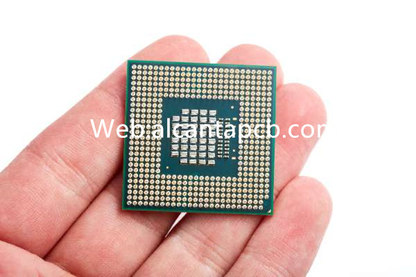
BGA semiconductores (Matriz de rejilla de bolas) El sustrato es una tecnología de embalaje de alta densidad que se utiliza ampliamente en el embalaje y conexión de circuitos integrados. (IM). Utiliza bolas de soldadura esféricas como medio de conexión., para que los chips de la placa de circuito se puedan conectar a la placa base u otros dispositivos a través de estas bolas de soldadura esféricas. En comparación con el embalaje tradicional con alfileres, Los sustratos BGA pueden lograr una mayor densidad de conexión y un mejor rendimiento eléctrico.
Los sustratos BGA suelen estar hechos de materiales semiconductores., como el silicio, arseniuro de galio (GaAs), etc.. Su estructura consta de chips., sustratos de embalaje, Conectores y bolas de soldadura esféricas.. Durante el proceso de fabricación, Los chips se empaquetan en un sustrato y se conectan mediante técnicas de soldadura.. Esta tecnología de embalaje permite que los sustratos BGA tengan mayor confiabilidad y mejores capacidades de gestión térmica., haciéndolos adecuados para una variedad de aplicaciones de dispositivos electrónicos de alto rendimiento.
Las principales características del sustrato BGA incluyen:
Conexión de alta densidad: Mediante tecnología de conexión de bola de soldadura esférica, El sustrato BGA puede lograr conexiones de mayor densidad., permitiendo acomodar más chips y dispositivos en la placa de circuito.
Excelente rendimiento eléctrico: El sustrato BGA tiene una ruta de transmisión de señal más corta y menor resistencia e inductancia., mejorando así el rendimiento y la estabilidad del circuito.
Buena gestión térmica: Debido al buen contacto entre las bolas de soldadura y el sustrato., El sustrato BGA puede transferir y dispersar más eficazmente el calor generado por el chip., reduciendo el estrés térmico del chip y mejorando la confiabilidad del sistema.
En general, El sustrato semiconductor BGA es una tecnología de embalaje avanzada que proporciona soluciones estables y de alto rendimiento para el diseño y fabricación de equipos electrónicos.. Con el continuo desarrollo y progreso de la industria electrónica., Los sustratos BGA seguirán desempeñando un papel importante, promoviendo la innovación continua de la tecnología y la expansión de aplicaciones.
¿Cuál es el proceso de fabricación de sustratos semiconductores BGA??
El proceso de fabricación de sustratos semiconductores BGA implica varios pasos clave, Cada paso es crucial y afecta la calidad y el rendimiento del producto final.. Estos pasos clave se detallan a continuación.:
Diseño: El primer paso en la fabricación de un sustrato semiconductor BGA es el diseño.. En esta etapa, el fabricante trabaja con el cliente para determinar las especificaciones, dimensiones, y disposición del sustrato. El equipo de diseño utiliza software CAD para diseñar y garantizar que el cableado y la disposición del conector del sustrato cumplan con los requisitos del producto..
Selección de material: La selección de materiales semiconductores de alto rendimiento adecuados para una aplicación específica es un paso crítico en el proceso de fabricación.. Estos materiales incluyen materiales de sustrato., materiales de embalaje, alambres metálicos, etc.. Los fabricantes seleccionarán los materiales apropiados en función de los requisitos del producto y los indicadores de rendimiento para garantizar la estabilidad y confiabilidad del sustrato..
Procesamiento de gráficos e imágenes.: El fabricante importará la imagen del sustrato BGA diseñada al software de procesamiento de imágenes y gráficos., y realizar varios ajustes y optimizaciones de parámetros para garantizar que la imagen final pueda reflejar con precisión los requisitos de diseño.
Fotolitografía: Durante el proceso de fabricación, La fotolitografía se utiliza para transferir patrones diseñados a la superficie del sustrato.. La fotolitografía es un proceso preciso que utiliza resina fotosensible y fotoprotector para proyectar patrones sobre la superficie de un sustrato y realizar los tratamientos químicos correspondientes para formar el patrón deseado..
Aguafuerte: Después de la fotolitografía, Se requiere un proceso de grabado para eliminar partes no deseadas del material de la superficie del sustrato., dejando los patrones y conectores deseados. El grabado puede utilizar métodos como el grabado químico o el grabado físico., Y el proceso de grabado apropiado se puede seleccionar de acuerdo con diferentes materiales y requisitos de diseño..
Metalización: Una vez completado el grabado, la superficie del sustrato debe metalizarse para mejorar el rendimiento conductivo del conector. La metalización puede utilizar métodos como galvanoplastia o deposición química de vapor para depositar una capa de metal en la superficie de un sustrato para formar un conector conductor..
Embalaje: El empaquetado es el proceso de montar un chip de circuito integrado en un sustrato BGA.. Los fabricantes utilizan equipos sofisticados para unir los chips al sustrato y mantenerlos en su lugar mediante soldadura u otros métodos de fijación.. El proceso de empaquetado también incluye pasos como instalar un disipador de calor y llenar el pegamento de embalaje para mejorar la estabilidad y el rendimiento de disipación de calor del chip..
Pruebas y control de calidad: El último paso crítico son las pruebas rigurosas y el control de calidad del sustrato BGA fabricado.. Los fabricantes utilizan diversos equipos y métodos de prueba para probar el rendimiento de los sustratos y garantizar que cumplan con los requisitos y estándares del producto.. Solo los sustratos que pasen la prueba podrán entregarse a los clientes para su uso..
Para resumir, El proceso de fabricación de sustratos semiconductores BGA incluye múltiples pasos clave, como el diseño., selección de material, procesamiento de gráficos e imágenes, fotolitografía, aguafuerte, metalización, embalaje, pruebas y control de calidad. Cada paso requiere equipos sofisticados y soporte técnico para garantizar que la calidad y el rendimiento del producto final cumplan con los requisitos y expectativas del cliente..
¿Cuáles son las ventajas de los sustratos semiconductores BGA en comparación con otros sustratos??
Los sustratos semiconductores BGA tienen muchas ventajas sobre otros sustratos, lo que los convierte en una de las tecnologías de embalaje preferidas en el campo de la electrónica actual..
Primero, el sustrato semiconductor BGA tiene mayor densidad. El sustrato BGA utiliza tecnología de conexión de matriz de rejilla de bolas. Comparado con los métodos de envasado tradicionales, sus puntos de conexión son más densos, para que pueda acomodar más conectores y chips en un espacio limitado. Esto hace que los sustratos BGA sean ideales para implementar diseños de circuitos integrados de alta densidad., especialmente para pequeños dispositivos electrónicos y aplicaciones de alto rendimiento.
En segundo lugar, El sustrato BGA tiene un rendimiento eléctrico superior y características de transmisión de señal.. Debido a la adopción de la tecnología de conexión de matriz de rejilla de bolas, Los sustratos BGA pueden proporcionar rutas de señal más cortas y menor resistencia e inductancia, reduciendo así el retraso y la pérdida de señal, y mejorar la estabilidad y confiabilidad de la transmisión de señales. Esto es particularmente importante para aplicaciones que requieren transmisión de datos de alta velocidad y bajo consumo de energía., como equipos de comunicación, ordenadores y electrónica de consumo.
Además, Los sustratos semiconductores BGA tienen mejores propiedades de gestión térmica.. El diseño del sustrato BGA le permite dispersar y disipar de manera más efectiva el calor generado por el chip., reduciendo así la temperatura del sistema y mejorando la eficiencia de disipación de calor. Esto es fundamental para que los chips de alto rendimiento y los dispositivos de larga duración garanticen la estabilidad y confiabilidad del sistema..
Además, Los sustratos BGA también tienen mayor confiabilidad y resistencia al impacto.. Porque su método de soldadura es más confiable y los puntos de conexión están encapsulados debajo del sustrato mediante una rejilla de bolas., Puede resistir mejor los golpes mecánicos y las vibraciones., Reducir la desconexión o los daños causados por factores ambientales externos.. Esto hace que los sustratos BGA se utilicen ampliamente en campos como el control industrial., electrónica automotriz, y aeroespacial, donde el equipo tiene requisitos extremadamente altos de confiabilidad y durabilidad.
Para resumir, El sustrato semiconductor BGA tiene muchas ventajas, como una mayor densidad., rendimiento eléctrico superior, mejor rendimiento de gestión térmica y mayor confiabilidad que otros sustratos. Estas ventajas hacen de los sustratos BGA la solución de embalaje preferida para diversos dispositivos electrónicos., Impulsando el continuo desarrollo y progreso de la industria electrónica..
¿En qué campos se utilizan los sustratos semiconductores BGA??
Los sustratos semiconductores BGA se utilizan ampliamente en el campo de la tecnología moderna y desempeñan un papel importante en diversos campos.. Las siguientes son varias áreas principales de aplicaciones de sustratos semiconductores BGA.:
En el campo de las comunicaciones electrónicas., Los sustratos semiconductores BGA se utilizan ampliamente en teléfonos móviles., equipo de comunicación por satélite, estaciones base de comunicación y otros equipos. Debido a su conexión de alta densidad y características de alto rendimiento, Los sustratos BGA pueden admitir sistemas de comunicación complejos y mejorar el rendimiento y la confiabilidad de los equipos de comunicación..
Los sustratos semiconductores BGA también se utilizan ampliamente en computadoras y equipos de red., incluyendo computadoras personales, servidores, enrutadores, interruptores, etc.. Los sustratos BGA proporcionan conexiones de circuitos estables y soluciones de embalaje, Apoyar el funcionamiento de alta velocidad de computadoras y equipos de red..
En el campo de la electrónica del automóvil., Los sustratos semiconductores BGA se utilizan en sistemas de control electrónico de automóviles., sistemas de entretenimiento para vehículos, sistemas de navegación, etc.. El sustrato BGA puede soportar los desafíos del entorno de trabajo automotriz y tiene alta resistencia al calor y a los golpes., Garantizar la estabilidad y confiabilidad de los equipos electrónicos automotrices..
Los sustratos semiconductores BGA también desempeñan un papel importante en los equipos médicos., incluyendo equipo de diagnóstico médico, equipo de monitoreo, equipo de imágenes médicas, etc.. Los sustratos BGA proporcionan soluciones de embalaje y conexión de circuitos precisas, Garantizar la precisión y confiabilidad de los equipos médicos y contribuir al desarrollo de la industria médica..
En el campo de la automatización industrial, Los sustratos semiconductores BGA se utilizan en equipos de automatización de fábricas., sistemas robóticos, sistemas de control de sensores, etc.. Los sustratos BGA presentan conexiones de alta densidad y alto rendimiento, y puede soportar sistemas complejos de automatización industrial y mejorar la eficiencia de la producción y la calidad del producto..
En general, Los sustratos semiconductores BGA se utilizan ampliamente en comunicaciones electrónicas., equipos informáticos y de red, electrónica automotriz, equipo medico, automatización industrial y otros campos. Su alto rendimiento y alta confiabilidad brindan soluciones de empaque y conexión de circuitos estables y eficientes para equipos en diversos campos., y promover el desarrollo y progreso de la tecnología moderna.
Cómo encontrar un fabricante de sustratos semiconductores BGA adecuado?
Para encontrar el fabricante de sustrato semiconductor BGA adecuado, es necesario considerar los siguientes factores:
Capacidades técnicas: Primero, es necesario evaluar las capacidades técnicas del fabricante. Esto incluye sus capacidades de diseño., procesos de fabricación, y sistemas de control de calidad. Asegúrese de que tengan suficiente experiencia y conocimientos para satisfacer las necesidades de su producto..
Capacidad de producción: La capacidad de producción del fabricante es otro factor importante.. Debe asegurarse de que tengan suficiente equipo de producción y recursos humanos para satisfacer las necesidades de su pedido., además de poder entregar productos de alta calidad a tiempo.
Estándares de calidad: La calidad es una de las consideraciones clave a la hora de elegir un fabricante.. Garantizar que los fabricantes cumplan con los estándares internacionales y las certificaciones de la industria., como ISO 9001 certificación del sistema de gestión de calidad, y otras certificaciones requeridas por los clientes.
Rentabilidad: además de calidad, La rentabilidad también es una de las consideraciones.. Debe evaluar si los precios del fabricante son razonables y compararlos con otros competidores.. Pero tenga en cuenta que elegir un precio bajo puede afectar la calidad del producto y los niveles de servicio..
Confiabilidad de la cadena de suministro: La confiabilidad de la cadena de suministro de un fabricante también es una consideración importante. Asegúrese de que su cadena de suministro sea estable y capaz de suministrar las materias primas requeridas de manera oportuna para no afectar su programa de producción..
Servicio y soporte: Finalmente, También desea considerar el servicio y soporte proporcionado por el fabricante.. Esto incluye soporte técnico., servicio postventa, y la capacidad de comunicarse y colaborar con los clientes.. Elija un fabricante que pueda brindar soporte integral, ayudarle a resolver los problemas encontrados durante el proceso de producción, y proporcionar soluciones personalizadas.
Para resumir, Encontrar un fabricante de sustrato semiconductor BGA adecuado requiere una consideración exhaustiva de factores como las capacidades técnicas., capacidades de producción, estándares de calidad, rentabilidad, confiabilidad de la cadena de suministro, y servicio y soporte. Evaluando cuidadosamente estos factores y comunicándose y trabajando plenamente con sus proveedores, Podrás encontrar el fabricante que mejor se adapta a las necesidades de tu empresa..
Cómo obtener una cotización para sustratos semiconductores BGA?
Obtener una cotización para un sustrato semiconductor BGA es un paso crítico, pero hay algunas cuestiones importantes a las que prestar atención al pasar por este proceso para garantizar que finalmente se seleccione el proveedor y el producto correctos.. Aquí hay algunos puntos a considerar.:
Antes de solicitar un presupuesto a un proveedor, asegúrese de tener claras las especificaciones completas para su proyecto. Esto incluye requisitos detallados para el tamaño., materiales, número de capas, tratamiento superficial, tamaño de apertura, ancho de línea y espacio entre líneas, etc.. Proporcionar especificaciones claras puede ayudar a los proveedores a comprender exactamente lo que necesita y cotizar en consecuencia..
Es muy importante determinar los requisitos de volumen del sustrato BGA que necesita.. En general, cantidades de pedidos más grandes obtendrán precios más competitivos. Por lo tanto, Es muy necesario proporcionar cantidades de pedido estimadas precisas cuando se consulta a los proveedores..
Comprender los plazos de entrega de su proveedor y los plazos de producción también es fundamental.. Los ciclos de producción de diferentes proveedores pueden variar., y esto afectará directamente el progreso de su proyecto. Por lo tanto, al elegir un proveedor, debe considerar sus capacidades de producción y si pueden cumplir con sus requisitos de tiempo.
Asegurar que los proveedores seleccionados tengan buenos sistemas de garantía de calidad y certificaciones relevantes.. Por ejemplo, ISO 9001 certificación del sistema de gestión de calidad, etc.. Esto puede garantizar que el sustrato BGA que compre sea de calidad confiable, estable y confiable.
Además de precio y calidad., El servicio y soporte del proveedor son igualmente importantes.. Esto incluye soporte técnico., servicio postventa, y la capacidad de responder rápidamente a los problemas. Al elegir un proveedor, es esencial considerar su nivel de servicio.
Asegúrese de que las cotizaciones proporcionadas por los proveedores sean claras y transparentes., incluyendo una descripción detallada de todos los costos. Esto puede ayudarlo a comprender mejor el origen de cada gasto en su cotización y realizar comparaciones y evaluaciones más precisas..
En general, obtener una cotización para un sustrato semiconductor BGA requiere una consideración exhaustiva del precio, calidad, el tiempo de entrega, soporte de servicio y otros aspectos. A través de plena comprensión y comunicación., Elegir el proveedor adecuado puede proporcionarle una solución de sustrato estable y confiable para su proyecto..
Preguntas frecuentes
¿Qué son los sustratos semiconductores BGA??
Sustratos semiconductores BGA, también conocido como sustratos Ball Grid Array, Son componentes esenciales en los dispositivos electrónicos., facilitar el empaquetado y la interconexión de circuitos integrados. Estos sustratos ofrecen capacidades de interconexión de alta densidad y un rendimiento eléctrico superior..
¿Qué papel juegan los fabricantes de sustratos semiconductores BGA??
Los fabricantes de sustratos semiconductores BGA son responsables del diseño., productor, y probar estos sustratos para cumplir con las especificaciones y requisitos de los dispositivos electrónicos. Garantizan la fiabilidad, actuación, y calidad de los sustratos BGA a través de procesos de fabricación avanzados y medidas de control de calidad..
¿Cómo se fabrican los sustratos semiconductores BGA??
El proceso de fabricación de sustratos semiconductores BGA implica varios pasos clave, incluyendo el diseño, selección de material, tratamiento, embalaje, y pruebas. Se utilizan tecnologías y equipos avanzados para fabricar sustratos con dimensiones precisas., estructuras, y propiedades electricas.
¿Qué ventajas ofrecen los sustratos semiconductores BGA sobre otros sustratos??
Los sustratos semiconductores BGA ofrecen varias ventajas, incluyendo interconexión de alta densidad, rendimiento eléctrico mejorado, gestión térmica mejorada, y confiabilidad superior. Estos sustratos permiten la integración de diseños de circuitos complejos en dispositivos electrónicos., contribuyendo a su funcionalidad y rendimiento.
¿En qué aplicaciones se utilizan comúnmente los sustratos semiconductores BGA??
Los sustratos semiconductores BGA encuentran aplicaciones generalizadas en diversos dispositivos electrónicos, incluyendo teléfonos inteligentes, tabletas, computadoras, electrónica automotriz, y más. Sirven como componentes críticos para empaquetar y conectar circuitos integrados en estos dispositivos., apoyando su funcionalidad y rendimiento.