CO., LTD")
Fabricante de PCB de antena ultrafina.”Fabricante de PCB de antena ultrafina” se especializa en la elaboración de placas de circuito impreso de última generación., Diseñado con las especificaciones más minuciosas para una recepción y transmisión de señal óptimas.. Con una combinación meticulosa de materiales avanzados e ingeniería de precisión., nuestras antenas cuentan con una delgadez incomparable, asegurando una integración perfecta incluso en los dispositivos más compactos sin sacrificar el rendimiento. Del concepto a la finalización, priorizamos la innovación, calidad, y confiabilidad, Atendiendo a diversas industrias como las telecomunicaciones., IoT, y aeroespacial. Experimente el futuro de la conectividad con nuestras soluciones personalizadas, donde lo ultradelgado se encuentra con lo ultrapotente, definiendo una nueva era en la tecnología inalámbrica.
¿Qué es la PCB de antena ultrafina??
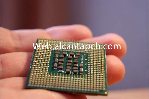
Antena ultrafina tarjeta de circuito impreso Es una placa de circuito impreso con un diseño extremadamente delgado cuya función principal es servir como elemento de antena en equipos de comunicación inalámbrica.. En comparación con los diseños de antena tradicionales, el diseño de PCB de antena ultradelgada es más compacto, permitiendo una transmisión y recepción de señales más eficiente, proporcionando conexiones confiables para varios dispositivos de comunicación inalámbrica.
En el campo de las comunicaciones inalámbricas., Las antenas son una parte importante de la transmisión y recepción de señales.. Los diseños de antenas tradicionales suelen requerir un gran espacio., lo que limita el diseño y aplicación de los equipos. La aparición de PCB de antena ultrafina ha cambiado esta situación.. Adopta tecnología avanzada de diseño y fabricación de miniaturización., permite integrar los elementos de la antena en la placa de circuito impreso y tiene una apariencia extremadamente delgada.
Debido a sus características de diseño ultradelgado, La PCB de antena ultrafina tiene amplias perspectivas de aplicación en varios dispositivos de comunicación inalámbrica. Por ejemplo, en dispositivos móviles como teléfonos inteligentes, tabletas, y relojes inteligentes, antena ultrafina PCB Puede lograr una mejor recepción y transmisión de señal., mejorar la calidad y velocidad de la comunicación, y proporcionar a los usuarios una mejor experiencia de usuario. Además, La PCB de antena ultrafina también se puede utilizar en dispositivos IoT, sistemas domésticos inteligentes, Sistemas de Internet de vehículos y otros campos., Proporcionar conexiones inalámbricas confiables para la interconexión de varios dispositivos inteligentes..
Además de su aplicación en equipos de comunicación inalámbrica tradicionales., La PCB de antena ultrafina también juega un papel importante en algunos escenarios especiales.. Por ejemplo, en el campo aeroespacial, El diseño miniaturizado de los PCB de antena ultradelgados puede cumplir con los estrictos requisitos de espacio y peso de las aeronaves y proporcionar un soporte confiable de transmisión de señales para los sistemas de navegación y comunicación de la aviación.. en equipos medicos, La aplicación de PCB de antena ultrafina puede realizar conexión inalámbrica y transmisión de datos de equipos médicos., proporcionando comodidad para el seguimiento y diagnóstico médico.
En general, La aparición de PCB de antena ultrafina ha traído nuevas oportunidades y desafíos al desarrollo de la tecnología de comunicación inalámbrica.. Su diseño extremadamente delgado, El rendimiento eficiente de la transmisión de señales y las amplias perspectivas de aplicación lo convierten en una parte indispensable e importante de la nueva generación de equipos de comunicación inalámbrica.. Con el continuo avance de la tecnología y la continua expansión de los campos de aplicación., Se cree que la PCB de antena ultrafina desempeñará un papel cada vez más importante en el futuro y promoverá el desarrollo continuo de la tecnología de comunicación inalámbrica..
Guía de referencia de diseño de PCB de antena ultrafina.
El diseño de la PCB de antena ultrafina es una parte crucial de los equipos de comunicación inalámbrica., y su diseño optimizado puede afectar directamente el rendimiento y estabilidad del equipo. Al diseñar una PCB de antena ultrafina, Hay varios factores clave que deben considerarse para garantizar un rendimiento óptimo de la antena..
Primero, Los diseñadores deben determinar el rango de frecuencia operativa y el ancho de banda de la antena en función de los escenarios de aplicación específicos y los requisitos del dispositivo.. Esto afectará directamente la estructura y el tamaño del diseño de la antena., y es necesario seleccionar la forma de antena adecuada según las diferentes frecuencias, como antenas de parche, conjuntos de antenas, etc..
En segundo lugar, El diseño y la disposición de las antenas también son consideraciones importantes en el diseño.. Un diseño razonable puede reducir la interferencia mutua entre antenas y mejorar el rendimiento de recepción y transmisión de las antenas.. Al mismo tiempo, También es necesario considerar la relación de diseño entre la antena y otros componentes del circuito para garantizar que la antena pueda trabajar junto con otros componentes para lograr un rendimiento óptimo del sistema..
La selección del material es otro factor crítico en el diseño de PCB de antena ultrafina. Es necesario seleccionar materiales con buenas propiedades dieléctricas y resistencia a altas frecuencias para garantizar la estabilidad y confiabilidad de la antena.. Los materiales comúnmente utilizados incluyen poliimida., poliamida, cerámica, etc., y el material apropiado se selecciona de acuerdo con los requisitos de aplicación específicos.
Además, El diseño de red correspondiente de la antena también es un aspecto que necesita atención en el diseño de PCB de antena ultrafina.. La red de adaptación puede mejorar el rendimiento de adaptación de la antena., hacer que se adapte mejor al entorno de trabajo en diferentes frecuencias de operación, y mejorar la eficiencia y cobertura de la transmisión de la señal.
Finalmente, Los diseñadores también necesitan utilizar herramientas de simulación para verificar y optimizar el plan de diseño para garantizar que el diseño de la antena cumpla con los indicadores de rendimiento y los requisitos del equipo.. La simulación puede evaluar rápidamente los pros y los contras de diferentes soluciones de diseño, Proporcionar una referencia para la posterior fabricación y prueba de prototipos..
Para resumir, El diseño de una PCB de antena ultrafina implica múltiples factores clave., incluido el rango de frecuencia, disposición del diseño, selección de material, diseño de red a juego, etc.. Los diseñadores deben considerar exhaustivamente estos factores., formular planes de diseño razonables, y garantizar el rendimiento óptimo de la antena mediante simulación, verificación y optimización., Brindar soporte técnico confiable para mejorar el rendimiento y expandir las aplicaciones de equipos de comunicación inalámbrica..
¿Qué material se utiliza en la PCB de antena ultrafina??
La PCB de antena ultrafina es un componente vital de los equipos de comunicación inalámbrica, y su selección de materiales es crucial, lo que afecta directamente la estabilidad y confiabilidad del rendimiento de la antena. Típicamente, Los PCB de antena ultradelgados utilizan materiales compuestos de alto rendimiento, incluyendo poliimida (PI) y poliamida (Pensilvania), para satisfacer las necesidades de diversos escenarios de aplicación.
Primero, Estos materiales tienen excelentes propiedades mecánicas., incluyendo alta resistencia, alta rigidez y buena resistencia al desgaste. Esta propiedad mecánica garantiza que la PCB de antena ultrafina no se deforme ni dañe fácilmente durante el uso y mantenga una buena estabilidad estructural., mejorando así la vida útil y la fiabilidad de la antena.
En segundo lugar, El material PCB de la antena ultrafina tiene una excelente resistencia a altas temperaturas y puede mantener un rendimiento eléctrico estable en entornos de alta temperatura.. Esto es particularmente importante para algunos escenarios de aplicación que necesitan funcionar en condiciones ambientales adversas., como sistemas de control industrial, Electrónica automotriz y otros campos., para garantizar que la antena pueda seguir funcionando normalmente en entornos de alta temperatura y no se vea afectada por la temperatura.
Además, Estos materiales también tienen una excelente resistencia química y pueden resistir la erosión de productos químicos como ácidos y álcalis., manteniendo la superficie de la antena lisa y limpia. Esta característica permite que la PCB de antena ultradelgada pueda hacer frente a diversos entornos de trabajo hostiles., como sitios de fabricación industrial, ambientes marinos, etc., asegurando que la antena funcione de manera estable durante mucho tiempo y no se vea afectada por el entorno externo.
En resumen, Las propiedades del material de los PCB de antena ultrafinos son cruciales y tienen un impacto significativo en el rendimiento y la confiabilidad de la antena.. El uso de materiales compuestos de alto rendimiento., como poliimida y poliamida, Puede garantizar que la antena tenga excelentes propiedades mecánicas., resistencia a altas temperaturas y resistencia a la corrosión química, satisfacer las necesidades de diversos escenarios de aplicación, y promover la innovación continua de la tecnología y el desarrollo de las comunicaciones inalámbricas..
¿De qué tamaño es la PCB de antena ultrafina??
La PCB de antena ultrafina desempeña un papel vital en los equipos de comunicación inalámbricos modernos. Su exquisito diseño y excelente rendimiento lo convierten en un componente indispensable de varios dispositivos.. Respecto a las dimensiones de las PCB de antena ultrafinas, generalmente varían de una aplicación a otra y pueden ser muy pequeños o más grandes, dependiendo de los requisitos de diseño del dispositivo y del rango de frecuencia de comunicación requerido.
En muchos dispositivos móviles, como teléfonos inteligentes, tabletas, y wearables, Los PCB de antena ultradelgados a menudo deben ser lo más pequeños posible para caber en el espacio reducido del dispositivo.. El tamaño de estos PCB suele oscilar entre unos pocos milímetros cuadrados y varios centímetros cuadrados., y su diseño delgado permite integrarlos fácilmente en la estructura interna del dispositivo sin ocupar demasiado espacio, al mismo tiempo que garantiza que el dispositivo sea liviano y portátil.
Por otro lado, para aplicaciones que requieren un mayor rendimiento y una cobertura más amplia, como enrutadores inalámbricos, estaciones base, y equipos de comunicación montados en vehículos, el tamaño de la PCB de la antena ultrafina puede ser mayor. Estos PCB pueden requerir áreas de superficie más grandes para acomodar estructuras de antena más complejas., así como más elementos de antena y conectores para una transmisión de señal más estable y confiable.
En general, Los PCB de antena ultradelgados están disponibles en una amplia gama de tamaños y pueden diseñarse a medida para satisfacer necesidades de aplicaciones específicas.. Ya sea en pequeños dispositivos móviles o grandes sistemas de comunicación, Los PCB de antena ultradelgados pueden brindar nuevas posibilidades al desarrollo y aplicación de la tecnología de comunicación inalámbrica con su diseño flexible y excelente rendimiento..
El proceso de fabricación de PCB de antena ultrafina.
El proceso de fabricación de PCB de antena ultrafina es un proceso complejo y preciso que implica múltiples pasos clave, incluida la preparación del sustrato, diseño de circuito, impresión, moldura, soldadura, y pruebas. Cada paso es crítico y tiene un impacto directo en la calidad y el rendimiento del producto final..
El primero es la preparación del sustrato.. En el proceso de fabricación de PCB de antena ultrafinas, seleccionar el material de sustrato adecuado es crucial. Típicamente, Los materiales compuestos de alto rendimiento, como la poliimida, se utilizan como materiales de sustrato porque tienen excelentes propiedades mecánicas., alta resistencia a la temperatura, y resistencia a la corrosión química, y puede cumplir con los requisitos de diseños ultrafinos. El proceso de preparación del sustrato incluye el corte del sustrato., Pasos para el tratamiento de la superficie y recubrimiento con lámina de cobre para garantizar que la superficie del sustrato sea plana y limpia para los procesos posteriores de diseño de circuitos e impresión..
Luego viene el diseño del circuito.. El diseño de circuitos de precisión es un eslabón clave en el proceso de fabricación de PCB de antena ultrafina. Optimizando la forma, Tamaño y diseño de la antena., una estructura de circuito que cumple con los requisitos está diseñada para lograr un mejor rendimiento de transmisión y recepción de la señal. Durante el proceso de diseño del circuito, factores como el rango de frecuencia, ganar, Es necesario considerar la directividad y la directividad de la antena para satisfacer las necesidades de diferentes escenarios de aplicación..
Luego viene la impresión y el moldeado.. Una vez completado el diseño del circuito, El diagrama de circuito diseñado se convierte en una placa de circuito impreso real.. Durante el proceso de impresión, Se utilizan equipos y tecnología de impresión avanzados para imprimir tinta conductora en la superficie del sustrato para formar una ruta conductora para la antena.. El proceso de moldeo implica procesar y dar forma a la placa de circuito impreso para garantizar que su tamaño y forma cumplan con los requisitos de diseño manteniendo al mismo tiempo el diseño ultrafino de la antena..
Luego viene la soldadura. Durante el proceso de soldadura, la placa de circuito está conectada a otros componentes electrónicos para formar un sistema de antena completo. La exquisitez de la tecnología de soldadura afecta directamente la estabilidad y confiabilidad de la antena.. Se requieren equipos y procesos de soldadura de precisión para garantizar que la calidad de la soldadura cumpla con los requisitos..
Por fin llega la prueba. Una vez finalizada la fabricación, La PCB de antena ultrafina se somete a rigurosas pruebas e inspecciones de calidad para garantizar que su rendimiento sea estable y confiable.. El contenido de la prueba incluye la respuesta de frecuencia., ganar, características de radiación y otros indicadores de la antena, así como pruebas funcionales de todo el sistema.. Solo pasando pruebas estrictas podemos garantizar que la calidad de la PCB de antena ultradelgada cumpla con los requisitos y pueda funcionar normalmente en diversos escenarios de aplicación..
En general, El proceso de fabricación de PCB de antena ultrafina requiere un alto grado de tecnología profesional y soporte de equipos sofisticados., y cada paso debe controlarse y gestionarse estrictamente para garantizar que la calidad y el rendimiento del producto final cumplan con los requisitos.. A través de la innovación tecnológica continua y la mejora de procesos, La PCB de antena ultradelgada podrá satisfacer mejor las cada vez más complejas y diversas necesidades de comunicación inalámbrica y promover el desarrollo y progreso continuo de la tecnología de comunicación inalámbrica..
El área de aplicación de la PCB de antena ultrafina.
La PCB de antena ultrafina desempeña un papel clave en el campo tecnológico actual. Sus áreas de aplicación cubren una amplia gama de equipos de comunicación inalámbrica., Proporcionar funciones confiables de conexión y transmisión de señales para el desarrollo de diversas industrias..
Las comunicaciones móviles son una de las principales áreas de aplicación de las PCB de antena ultrafinas. Con el continuo desarrollo de la tecnología de comunicación móvil., La demanda de teléfonos móviles por parte de la gente, tabletas y otros dispositivos móviles también está aumentando. El diseño de PCB de antena ultrafina puede lograr una mejor recepción y transmisión de señal, mejorar el rendimiento y la estabilidad de los equipos de comunicación, y proporcionar a los usuarios una experiencia de comunicación más fluida.
El Internet de las cosas es otra área de aplicación importante. Con la popularización de la tecnología IoT, Cada vez es necesario interconectar más dispositivos inteligentes.. El diseño ultradelgado y el excelente rendimiento de la PCB de antena ultradelgada la convierten en una opción ideal para diversos dispositivos IoT, permitiendo una transmisión de señal estable y confiable, proporcionando un fuerte apoyo para el desarrollo de aplicaciones de IoT.
El hogar inteligente es otra área de aplicación importante para la PCB de antena ultrafina. A medida que la demanda de productos para el hogar inteligente continúa aumentando, varios dispositivos inteligentes, como altavoces inteligentes, lámparas inteligentes, cámaras inteligentes, etc.. seguir surgiendo. El diseño de PCB de antena ultradelgada puede lograr un diseño compacto del dispositivo, mejorar la estética general y la experiencia del usuario del dispositivo, e inyectar nueva vitalidad al desarrollo de la industria del hogar inteligente.
Internet de los vehículos es también una de las áreas de aplicación importantes de la PCB de antena ultrafina.. Con el desarrollo continuo de la tecnología inteligente del automóvil., Cada vez más automóviles necesitan realizar una conexión en tiempo real con el entorno externo.. El excelente rendimiento de la PCB de antena ultrafina puede satisfacer los altos requisitos de los automóviles para la transmisión de señales., Garantizar que el equipo montado en el vehículo pueda seguir funcionando de forma estable cuando se conduce a altas velocidades., y proporcionar una base sólida para el desarrollo de la tecnología de Internet de los vehículos.
En general, La PCB de antena ultrafina se utiliza ampliamente en comunicaciones móviles., Internet de las cosas, hogar inteligente, Internet de Vehículos y otros campos, Proporciona funciones confiables de conexión y transmisión de señal para varios dispositivos de comunicación inalámbrica.. Su diseño ultrafino y su excelente rendimiento lo convierten en un componente clave de la nueva generación de tecnología de comunicación inalámbrica., Impulsar la innovación y el desarrollo continuos de la tecnología de comunicación inalámbrica..
¿Cuáles son las ventajas de la PCB de antena ultrafina??
Los PCB de antena ultradelgados ofrecen numerosas ventajas sobre los diseños de antena tradicionales que los convierten en una innovación importante en las comunicaciones inalámbricas.. Primero, El tamaño pequeño y el peso ligero de las PCB de antena ultrafinas les permiten ocupar menos espacio en diversos dispositivos electrónicos y permiten un diseño e instalación más flexibles.. Esto no sólo hace que el dispositivo sea más ligero y portátil, pero también proporciona una mayor libertad en el diseño del producto para satisfacer a los usuarios.’ diferentes necesidades de apariencia y tamaño del dispositivo.
En segundo lugar, el diseño de la PCB de antena ultrafina hace que la transmisión de señal sea más estable. Debido a su naturaleza ultrafina, la antena puede adaptarse mejor a la superficie del dispositivo, Reducir la interferencia y la pérdida de señal durante la transmisión de la señal.. Esto significa que los equipos de comunicación inalámbrica pueden lograr conexiones de señal más confiables., mejorar las velocidades de transmisión de datos y la calidad de la comunicación, y proporcionar a los usuarios una experiencia más estable y fluida.
Además, el diseño ultrafino de la PCB de antena ultrafina permite una mejor integración del dispositivo. Se pueden integrar estrechamente con otras placas de circuito y componentes., haciendo que todo el dispositivo sea más compacto y mejorando el rendimiento general y la confiabilidad del dispositivo. Esto no sólo ayuda a simplificar el proceso de fabricación y el proceso de montaje del equipo., pero también reduce los costos de producción y mejora la eficiencia de la producción..
En general, La PCB de antena ultrafina tiene ventajas obvias en términos de volumen., peso, estabilidad de transmisión de señal, e integración de dispositivos. Su diseño ultradelgado no sólo puede cumplir con los requisitos de tamaño y peso de los equipos electrónicos modernos., sino que también mejora el rendimiento y la confiabilidad de los equipos de comunicación inalámbrica, proporcionando a los usuarios una mejor experiencia de usuario. Con el desarrollo continuo de la tecnología de comunicación inalámbrica y la expansión de los campos de aplicación., La PCB de antena ultrafina sin duda desempeñará un papel cada vez más importante en el futuro..
Preguntas frecuentes
¿Cuáles son las ventajas de las PCB de antena ultrafinas sobre los diseños de antena tradicionales??
En comparación con los diseños de antena tradicionales, PCB de antena ultrafina tiene las ventajas de un tamaño pequeño, peso ligero, y transmisión de señal estable. Su diseño compacto permite una mejor integración de los equipos y al mismo tiempo reduce el uso de espacio.. Además, El diseño optimizado de la antena y la selección de materiales pueden mejorar la estabilidad y confiabilidad de la transmisión de la señal., Permitir a los usuarios tener una mejor experiencia al utilizar dispositivos de comunicación inalámbrica..
¿Cuáles son las consideraciones de selección de materiales para PCB de antena ultrafinas??
Al seleccionar materiales para PCB de antena ultrafinas, es necesario considerar varios factores, incluyendo las propiedades mecánicas del material, alta resistencia a la temperatura, resistencia química, y costo. Los materiales comúnmente utilizados incluyen materiales compuestos de alto rendimiento como poliimida y poliamida., que tienen excelentes propiedades físicas y químicas y pueden satisfacer las necesidades de funcionamiento de antenas en diferentes entornos.
¿Cuáles son los pasos clave en el proceso de fabricación de PCB de antena ultrafina??
El proceso de fabricación de PCB de antena ultrafina incluye varios pasos, como la preparación del sustrato., diseño de circuito, impresión, moldura, soldadura y prueba. Entre ellos, El diseño de circuitos de precisión y la tecnología de fabricación son la clave para garantizar un rendimiento estable de la antena., y se requieren equipos y tecnología avanzados para lograr un procesamiento y ensamblaje de alta precisión.
¿En qué campos se utilizan principalmente los PCB de antena ultrafinos??
La PCB de antena ultrafina se utiliza ampliamente en comunicaciones móviles, Internet de las cosas, hogar inteligente, Internet de Vehículos y otros campos. Proporciona funciones confiables de conexión y transmisión de señal para varios dispositivos de comunicación inalámbrica., y promueve la innovación y el desarrollo continuos de la tecnología de comunicación inalámbrica. Ya sean teléfonos inteligentes, relojes inteligentes, Dispositivos domésticos inteligentes y sistemas de comunicación para vehículos., Se puede utilizar tecnología PCB de antena ultrafina..
¿Cuál es la tendencia de desarrollo futuro de la PCB de antena ultrafina??
Con el desarrollo continuo de la tecnología de comunicación inalámbrica y la popularización de los dispositivos inteligentes., La tecnología de PCB de antena ultrafina marcará el comienzo de perspectivas de aplicación más amplias. En el futuro, Las personas tendrán requisitos cada vez mayores en cuanto al tamaño y peso de los equipos de comunicación., y la PCB de antena ultrafina se convertirá en una de las tecnologías clave para satisfacer esta demanda. Al mismo tiempo, con la continua innovación de materiales y procesos de fabricación, El rendimiento y la confiabilidad de los PCB de antena ultradelgados seguirán mejorando., Proporcionar un mayor apoyo al desarrollo de la tecnología de comunicación inalámbrica..