CO., LTD")
Ultrafino Sustratos BGA Fabricante. Somos un fabricante líder de sustratos BGA ultrafinos., especializada en producir alto rendimiento, Soluciones miniaturizadas para aplicaciones electrónicas avanzadas.. Nuestros procesos de fabricación de última generación garantizan una calidad y confiabilidad superiores., Satisfacer las demandas de la tecnología moderna en industrias como las telecomunicaciones., computación, y electrónica de consumo.
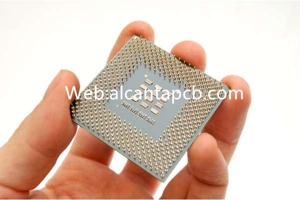
Matriz de rejilla de bolas ultrafina (BGA) sustratos Son componentes esenciales en el embalaje de circuitos integrados. (IM), particularmente en aplicaciones de alta densidad y alto rendimiento. Estos sustratos ofrecen un rendimiento eléctrico y térmico superior al tiempo que minimizan el tamaño y el peso total del paquete electrónico.. Los sustratos BGA ultrafinos se utilizan cada vez más en electrónica avanzada, como teléfonos inteligentes, computadoras portátiles, y otros dispositivos portátiles, donde el espacio y el rendimiento son consideraciones críticas.
¿Qué es un sustrato BGA ultrafino??
Un sustrato BGA ultrafino es un tipo de sustrato utilizado en el embalaje de dispositivos semiconductores.. Sirve como base sobre la cual se monta el chip semiconductor y proporciona las conexiones eléctricas necesarias entre el chip y la placa de circuito impreso. (tarjeta de circuito impreso). El “ultrafino” El aspecto se refiere al espesor reducido del sustrato en comparación con los sustratos BGA tradicionales., permitiendo paquetes electrónicos más compactos y livianos.
El empaque BGA implica colocar bolas de soldadura en un patrón de cuadrícula en la superficie inferior del sustrato., que se utilizan para crear conexiones eléctricas a la PCB durante el proceso de soldadura por reflujo. Los sustratos BGA ultrafinos mantienen la misma funcionalidad pero ofrecen un espesor reducido, haciéndolos ideales para aplicaciones donde el espacio es un bien escaso.
Guía de referencia de diseño de sustrato BGA ultrafino
El diseño de un sustrato BGA ultrafino implica varias consideraciones clave para garantizar un rendimiento y una fiabilidad óptimos.. Las siguientes secciones describen los aspectos esenciales del diseño de sustrato BGA ultrafino..
Se deben abordar varias consideraciones clave durante la fase de diseño.:
Control de impedancia: El control preciso de la impedancia es esencial para mantener la integridad de la señal en altas frecuencias.. Esto implica un diseño cuidadoso de las trazas de señal y el uso de materiales de impedancia controlada..
Gestión térmica: La gestión térmica eficaz es crucial para aplicaciones de alta potencia. El diseño debe incorporar vías térmicas., disipadores de calor, u otras técnicas para disipar eficientemente el calor.
Estabilidad mecánica: El sustrato debe proporcionar un soporte mecánico robusto para resistir los ciclos térmicos y las tensiones mecánicas durante el funcionamiento..
Fiabilidad: La confiabilidad a largo plazo está garantizada mediante el uso de materiales de alta calidad y procesos de fabricación precisos., evitando problemas como la delaminación y la deformación.
¿Qué materiales se utilizan en los sustratos BGA ultrafinos??
Los materiales utilizados en los sustratos BGA ultrafinos se seleccionan por sus propiedades complementarias para mejorar el rendimiento general del sustrato.:
Laminados de alto rendimiento: Proporciona resistencia mecánica y estabilidad térmica manteniendo un perfil delgado.. Los materiales comunes incluyen poliimida., polímero de cristal líquido (LCP), y FR-4 de alta temperatura.
Láminas de cobre ultrafinas: Utilizado para las capas conductoras., proporcionando excelente conductividad eléctrica y confiabilidad.
Dieléctricos de bajas pérdidas: Se utiliza para aislar las pistas conductoras y mantener la integridad de la señal..
Adhesivos avanzados: Une las capas y proporciona estabilidad mecánica..
¿De qué tamaño son los sustratos BGA ultrafinos??
El tamaño de los sustratos BGA ultrafinos varía según la aplicación y los requisitos de diseño específicos.:
Espesor: Los sustratos BGA ultrafinos suelen tener un espesor que oscila entre 50 a 200 micrómetros, dependiendo de los requisitos de diseño y aplicación.
Dimensiones: La longitud y el ancho de los sustratos están determinados por el tamaño de la matriz semiconductora y el diseño del sistema.. Pueden variar desde factores de forma pequeños para dispositivos compactos hasta sustratos más grandes para sistemas electrónicos más complejos..
El proceso de fabricación de sustratos BGA ultrafinos
El proceso de fabricación de sustratos BGA ultrafinos implica varios pasos precisos y controlados para garantizar una alta calidad y rendimiento.:
Laminados de alta calidad, láminas de cobre, y los adhesivos se seleccionan y preparan para su procesamiento.. Los materiales se limpian y tratan para eliminar cualquier impureza y garantizar una superficie lisa..
Las capas del sustrato se laminan entre sí mediante calor y presión.. Este paso garantiza que las capas estén unidas de forma segura y que el sustrato mantenga su perfil delgado..
Las capas conductoras están modeladas y grabadas para crear las vías eléctricas necesarias.. Esto implica el uso de técnicas de fotolitografía y grabado químico para lograr patrones precisos y exactos..
Se perforan agujeros en el sustrato para crear vías para las conexiones eléctricas entre las capas.. Luego, las vías se recubren con cobre para garantizar una conductividad eléctrica confiable..
Las bolas de soldadura se colocan en un patrón de cuadrícula en la superficie inferior del sustrato.. Estas bolas se utilizarán para crear conexiones eléctricas a la PCB durante el proceso de soldadura por reflujo..
Después de la fabricación, El sustrato se ensambla con la matriz semiconductora y todos los componentes y conectores necesarios.. Se realizan pruebas rigurosas para garantizar que el sustrato cumpla con todas las especificaciones de diseño y requisitos de rendimiento.. Esto incluye pruebas de rendimiento eléctrico., gestión térmica, e integridad mecánica.
El área de aplicación de los sustratos BGA ultrafinos
Los sustratos BGA ultrafinos se utilizan en una amplia gama de aplicaciones de alto rendimiento:
En dispositivos móviles como smartphones y tablets, Los sustratos BGA ultrafinos proporcionan el rendimiento necesario y el tamaño compacto para admitir funcionalidades avanzadas y al mismo tiempo minimizar el grosor general del dispositivo..
En electrónica portátil, Los sustratos BGA ultrafinos permiten la integración de funciones avanzadas en factores de forma compactos y livianos., garantizando comodidad y facilidad de uso para el usuario.
En aplicaciones informáticas de alto rendimiento, Los sustratos BGA ultrafinos proporcionan el rendimiento eléctrico y térmico necesario para soportar las capacidades de procesamiento avanzadas de las CPU y GPU modernas..
En equipos de telecomunicaciones, Los sustratos BGA ultrafinos se utilizan para soportar los requisitos de alta frecuencia y alta potencia de los sistemas de comunicación avanzados..
En electrónica automotriz, Los sustratos BGA ultrafinos proporcionan la confiabilidad y el rendimiento necesarios para los sistemas avanzados de asistencia al conductor. (ADA) y otros sistemas electrónicos en vehículos.
¿Cuáles son las ventajas de los sustratos BGA ultrafinos??
Los sustratos BGA ultrafinos ofrecen varias ventajas que los hacen indispensables en aplicaciones de alto rendimiento:
Tamaño compacto: Los sustratos BGA ultrafinos permiten el diseño de paquetes electrónicos compactos y livianos, ideal para aplicaciones portátiles y con espacio limitado.
Alto rendimiento eléctrico: Los sustratos BGA ultrafinos proporcionan un excelente rendimiento eléctrico con una mínima pérdida de señal y una alta integridad de la señal..
Gestión térmica eficiente: Los sustratos BGA ultrafinos proporcionan una gestión térmica eficiente, disipar el calor de manera efectiva y mantener el rendimiento de los componentes de alta potencia.
Estabilidad mecánica: Los sustratos BGA ultrafinos ofrecen un soporte mecánico robusto, Soportar ciclos térmicos y tensiones mecánicas durante el funcionamiento..
Versatilidad: Los sustratos BGA ultrafinos se pueden utilizar en una amplia gama de aplicaciones, desde dispositivos móviles hasta informática de alto rendimiento y electrónica automotriz.
Preguntas frecuentes
¿Cuáles son las consideraciones clave al diseñar un sustrato BGA ultrafino??
Las consideraciones clave incluyen la selección de materiales para el rendimiento térmico y eléctrico., Apilamiento de capas para integridad de la señal y gestión térmica., y garantizar la estabilidad mecánica y la fiabilidad..
¿En qué se diferencian los sustratos BGA ultrafinos de los sustratos BGA tradicionales??
Los sustratos BGA ultrafinos tienen un espesor reducido en comparación con los sustratos BGA tradicionales, permitiendo paquetes electrónicos más compactos y livianos manteniendo la misma funcionalidad.
¿Cuál es el proceso de fabricación típico de sustratos BGA ultrafinos??
El proceso implica la preparación del material., laminación de capas, modelado y grabado, taladrado y enchapado, accesorio de bola de soldadura, y montaje y pruebas rigurosos para garantizar una alta calidad y rendimiento..
¿Cuáles son las principales aplicaciones de los sustratos BGA ultrafinos??
Los sustratos BGA ultrafinos se utilizan en dispositivos móviles, electrónica portátil, informática de alto rendimiento, equipo de telecomunicaciones, y electrónica automotriz, Proporciona funcionalidad avanzada y confiabilidad en factores de forma compactos..