CO., LTD")
CI ultrafino Sustratos de paquete Fabricante. Somos un fabricante líder de sustratos de paquetes de circuitos integrados ultrafinos., proporcionando soluciones de vanguardia para dispositivos electrónicos de alto rendimiento. Nuestras técnicas de fabricación avanzadas garantizan una calidad excepcional., permitiendo la miniaturización y la funcionalidad mejorada en diversas aplicaciones, desde teléfonos inteligentes hasta dispositivos médicos. Confíe en nosotros para innovación, confiable, y sustratos de paquetes de circuitos integrados eficientes que satisfacen las demandas del mundo actual impulsado por la tecnología.
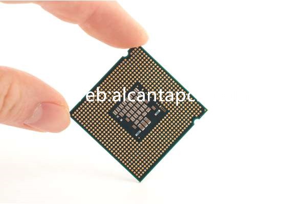
CI ultrafino (Circuito Integrado) paquete sustratos Son un componente vital en la electrónica moderna., permitiendo la miniaturización y el rendimiento mejorado de varios dispositivos. Estos sustratos están diseñados para ser extremadamente delgados y al mismo tiempo mantener la electricidad necesaria., térmico, y propiedades mecánicas para soportar circuitos integrados de alto rendimiento. Los sustratos ultrafinos son particularmente importantes en aplicaciones donde el espacio es escaso, como teléfonos inteligentes, dispositivos portátiles, y sistemas informáticos avanzados.
¿Qué es un sustrato de paquete de circuitos integrados ultrafino??
Un sustrato de paquete de circuitos integrados ultrafino es un tipo especializado de placa de circuito impreso. (tarjeta de circuito impreso) Diseñado para proporcionar una plataforma para montar e interconectar circuitos integrados.. Estos sustratos se caracterizan por su mínimo espesor., normalmente menos de 100 micrómetros, que permite el desarrollo de paquetes electrónicos ultracompactos. A pesar de su delgadez, Los sustratos ultrafinos deben soportar interconexiones de alta densidad., gestión térmica eficiente, y estabilidad mecánica robusta para garantizar el funcionamiento confiable de los circuitos integrados que albergan.
Guía de referencia de diseño de sustrato del paquete de circuitos integrados ultradelgados
El diseño de sustratos de paquetes de circuitos integrados ultrafinos implica un enfoque integral para garantizar un rendimiento y una confiabilidad óptimos..
La selección de materiales es fundamental para lograr las propiedades deseadas en sustratos ultrafinos.:
Películas de poliimida de alta densidad: Estos materiales ofrecen una excelente flexibilidad., alta estabilidad térmica, y buen aislamiento eléctrico, haciéndolos ideales para aplicaciones ultrafinas.
Láminas de cobre: Utilizado para trazas conductoras e interconexiones., Las láminas de cobre deben ser delgadas pero duraderas para mantener el rendimiento eléctrico sin agregar un volumen significativo..
Adhesivos y Dieléctricos: Se utilizan adhesivos avanzados y materiales dieléctricos con constantes dieléctricas bajas y alta conductividad térmica para unir las capas y proporcionar aislamiento..
La estructura de capas de los sustratos ultrafinos está diseñada para maximizar la eficiencia y el rendimiento del espacio.:
Capas de señal: Estas capas están configuradas para minimizar la pérdida de señal y la diafonía.. Se utilizan técnicas como microstrip y stripline para mantener la impedancia controlada..
Capas de energía y tierra: Los planos de tierra y energía dedicados son cruciales para una distribución estable de energía y reducción de ruido., asegurando un funcionamiento confiable del IC.
Capas de gestión térmica: La integración de vías térmicas y disipadores de calor ayuda a disipar el calor de manera efectiva, evitando el sobrecalentamiento de componentes críticos.
Capas de interconexión: Interconexiones de alta densidad (IDH) con microvías y orificios pasantes que permiten un enrutamiento complejo dentro del espacio limitado de sustratos ultrafinos.
¿Qué materiales se utilizan en los sustratos de paquetes de circuitos integrados ultrafinos??
Los materiales utilizados en los sustratos de paquetes de circuitos integrados ultrafinos se seleccionan por su capacidad para cumplir con estrictos requisitos de rendimiento.:
Películas de poliimida de alta densidad: Ofreciendo una excelente flexibilidad, estabilidad térmica, y aislamiento eléctrico, Estas películas son una opción común para aplicaciones ultrafinas..
Láminas de cobre: Se utilizan láminas de cobre finas pero duraderas para trazas conductoras e interconexiones., asegurando un rendimiento eléctrico confiable.
Adhesivos y Dieléctricos: Se utilizan adhesivos avanzados y materiales dieléctricos con constantes dieléctricas bajas y alta conductividad térmica para unir las capas y proporcionar aislamiento..
Resinas Epoxi Reforzadas: Estos materiales mejoran la resistencia mecánica del sustrato manteniendo un perfil bajo..
¿De qué tamaño son los sustratos del paquete de circuitos integrados ultrafinos??
El tamaño de los sustratos del paquete de circuitos integrados ultrafinos varía según la aplicación específica y los requisitos del dispositivo.:
Espesor: Los sustratos ultrafinos suelen tener menos de 100 micrómetros de espesor, Algunos diseños alcanzan espesores aún más bajos para adaptarse a los factores de forma más pequeños..
Largo y ancho: Estas dimensiones están determinadas por el tamaño del IC y el diseño de las interconexiones.. Los tamaños típicos varían desde unos pocos milímetros para circuitos integrados pequeños hasta varios centímetros para paquetes más grandes..
El proceso de fabricación de sustratos de paquetes de circuitos integrados ultrafinos
El proceso de fabricación de sustratos de paquetes de circuitos integrados ultrafinos implica varios pasos precisos y controlados para garantizar una alta calidad y rendimiento.:
Películas de poliimida de alta densidad., materiales conductores, y los adhesivos se preparan y cortan en tamaños apropiados para su procesamiento..
Las capas se fabrican laminando materiales conductores y aislantes en una pila.. Cada capa tiene un patrón mediante fotolitografía para definir los circuitos..
Las microvías y los orificios pasantes se perforan mediante técnicas de perforación láser o mecánica.. Luego, estos orificios se recubren con cobre para crear conexiones eléctricas entre capas..
Se utilizan procesos de fotolitografía y grabado para crear circuitos de paso fino en cada capa.. Este paso requiere alta precisión para garantizar interconexiones precisas y confiables..
Después de la fabricación de capas, las capas se laminan juntas bajo calor y presión. El sustrato ensamblado se somete a rigurosas pruebas., incluyendo pruebas eléctricas, ciclo térmico, y pruebas de estrés mecánico, para garantizar el rendimiento y la confiabilidad.
El área de aplicación de sustratos de paquetes de circuitos integrados ultrafinos
Los sustratos de paquetes de circuitos integrados ultrafinos permiten capacidades avanzadas en una amplia gama de aplicaciones:
En teléfonos inteligentes, tabletas, y dispositivos portátiles, Los sustratos ultrafinos admiten la integración compacta y eficiente de circuitos integrados avanzados., Mejorar el rendimiento y la funcionalidad al tiempo que reduce el tamaño y el peso..
en servidores, centros de datos, y supercomputadoras, Los sustratos ultrafinos permiten la integración de potentes procesadores y módulos de memoria en un formato compacto., facilitar el procesamiento y almacenamiento rápido de datos.
Estos sustratos son esenciales en infraestructuras de telecomunicaciones, incluidas estaciones base y equipos de red, proporcionando conectividad confiable y de alta velocidad en un espacio compacto.
En diversos productos electrónicos de consumo., desde dispositivos domésticos inteligentes hasta consolas de juegos, Los sustratos ultrafinos permiten un alto rendimiento en elegantes, diseños que ahorran espacio.
En equipos de diagnóstico e imágenes médicas., Los sustratos ultrafinos admiten la adquisición y el procesamiento de datos a alta velocidad., mejorar la precisión y la eficiencia en los procedimientos médicos.
¿Cuáles son las ventajas de los sustratos de paquetes de circuitos integrados ultrafinos??
Los sustratos de paquetes de circuitos integrados ultrafinos ofrecen varias ventajas que los hacen indispensables para aplicaciones electrónicas avanzadas.:
Diseño compacto: El perfil ultrafino permite la miniaturización de paquetes electrónicos., permitiendo dispositivos más compactos y portátiles.
Rendimiento alto: Los materiales y el diseño optimizados garantizan una alta integridad de la señal, baja pérdida de energía, y gestión térmica eficaz.
Fiabilidad mejorada: Los procesos y materiales de fabricación avanzados proporcionan una alta confiabilidad., Garantizar el rendimiento a largo plazo en entornos exigentes..
Flexibilidad: La naturaleza delgada y flexible de estos sustratos los hace adecuados para una amplia gama de aplicaciones., desde dispositivos rígidos de alto rendimiento hasta dispositivos electrónicos flexibles y portátiles.
Escalabilidad: Los sustratos ultrafinos se pueden personalizar para satisfacer las necesidades específicas de diversas aplicaciones., desde pequeños dispositivos de consumo hasta grandes sistemas industriales.
Preguntas frecuentes
¿Cuáles son las consideraciones clave al diseñar sustratos de paquetes de circuitos integrados ultrafinos??
Las consideraciones clave incluyen la selección de materiales para las propiedades eléctricas y térmicas., optimización de la estructura de capas para la integridad de la señal y la gestión térmica, y garantizar la estabilidad mecánica y la fiabilidad..
¿En qué se diferencian los sustratos de paquetes de circuitos integrados ultrafinos de los PCB estándar??
Los sustratos de paquetes de circuitos integrados ultrafinos son significativamente más delgados, con más capas y mayor densidad de interconexión, Diseñado para manejar frecuencias y niveles de potencia más altos en comparación con los PCB estándar., haciéndolos adecuados para aplicaciones avanzadas.
¿Cuál es el proceso de fabricación típico para sustratos de paquetes de circuitos integrados ultrafinos??
El proceso implica la preparación del material., fabricación de capas, taladrado y enchapado, modelado de circuitos, asamblea, y pruebas rigurosas para garantizar un alto rendimiento y confiabilidad.
¿Cuáles son las principales aplicaciones de los sustratos de paquetes de circuitos integrados ultrafinos??
Estos sustratos se utilizan en dispositivos móviles., informática de alto rendimiento, telecomunicaciones, electrónica de consumo, y dispositivos médicos, proporcionando funcionalidad avanzada y confiabilidad en estos campos.