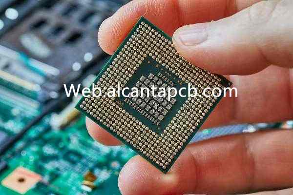
ABF GL102R8HF Package Substrates Manufacturer.As a leading ABF GL102R8HF Package Substrates manufacturer, we specialize in producing high-performance substrates designed for advanced semiconductor applications. Our products ensure superior signal integrity, efficient heat dissipation, and robust mechanical support. With cutting-edge technology and stringent quality control, we deliver reliable solutions that meet the evolving demands of the electronics industry.
ABF (Ajinomoto Build-up Film) GL102R8HF package substrates are cutting-edge materials used in advanced semiconductor packaging. These substrates play a crucial role in supporting the high-density interconnects and enhanced performance required for modern electronic devices. This article delves into the properties, structure, materials, manufacturing processes, applications, advantages, and frequently asked questions (FAQs) related to ABF GL102R8HF package substrates.
Structure of ABF GL102R8HF Package Substrates
The structure of ABF GL102R8HF package substrates is meticulously designed to meet the demanding requirements of high-performance semiconductor devices:

ABF GL102R8HF is a high-performance epoxy resin film known for its excellent electrical insulation, mechanical strength, and thermal stability. It serves as the primary dielectric material in the substrate.
Multiple layers of copper are used for electrical connections. These layers are finely patterned to achieve high-density interconnects essential for advanced semiconductor applications.
A designated area on the substrate where the semiconductor die is attached using adhesives or solder. This area must provide excellent thermal conductivity to dissipate heat generated by the IC.
Specific areas on the substrate designed for wire bonding or flip-chip bonding. These pads are typically coated with a finish such as gold to enhance bondability and prevent oxidation.
High-performance dielectric materials, such as ABF GL102R8HF, separate the conductive layers, ensuring electrical isolation and maintaining signal integrity.
Microvias and through-hole vias are used to create vertical interconnections between the different layers of the substrate, enabling high-density routing and minimizing parasitic inductance and capacitance.
Various surface finishes, such as ENIG (Electroless Nickel Immersion Gold) or OSP (Organic Solderability Preservatives), are applied to protect copper surfaces and enhance solderability.
Materials Used in ABF GL102R8HF Package Substrates
Key materials used in ABF GL102R8HF package substrates include:
A high-performance epoxy resin film with excellent electrical insulation properties, high glass transition temperature, and good adhesion to copper, making it ideal for high-density interconnects and advanced semiconductor applications.
High-purity copper is used for conductive traces due to its superior electrical conductivity and reliability.
Low dielectric constant and low loss tangent materials are essential for maintaining high signal integrity and minimal signal loss.
Surface finishes like ENIG and OSP are used to protect the copper traces from oxidation and enhance solderability.
Manufacturing Process of ABF GL102R8HF Package Substrates
The manufacturing process for ABF GL102R8HF package substrates involves several precise steps to ensure high performance and reliability:
Choosing appropriate base materials and conductive layers based on performance requirements.
Building up multiple layers of conductive and dielectric materials using ABF GL102R8HF film, forming a stable substrate with reduced thickness and enhanced performance.
Precision drilling, including laser drilling, is used to create microvias and through-holes for vertical interconnections.
Electroplating copper onto the substrate and inside vias to establish reliable electrical connections.
Using photolithography and chemical etching to define the circuit patterns and interconnects.
Applying protective coatings to exposed copper surfaces to enhance solderability and protect against oxidation.
Attaching the semiconductor die to the substrate using advanced flip-chip or wire bonding techniques, ensuring minimal signal loss and distortion.
Encapsulating the die for mechanical protection and thermal stability, followed by rigorous testing for electrical performance, signal integrity, and adherence to design specifications.
Applications of ABF GL102R8HF Package Substrates
ABF GL102R8HF package substrates are used in a wide range of high-performance applications, including:
Smartphones, tablets, and other portable devices that require compact and high-performance IC packaging.
Base stations, network equipment, and other communication devices that demand high-frequency signal transmission and reliable connections.
Advanced driver-assistance systems (ADAS), infotainment systems, and other electronic components in vehicles.
High-performance computing and control systems used in manufacturing and process automation.
Diagnostic and imaging equipment that require high reliability and precision.
Advantages of ABF GL102R8HF Package Substrates
ABF GL102R8HF package substrates offer several significant advantages:
The use of ABF GL102R8HF film allows for the creation of high-density interconnects, enabling advanced semiconductor designs and increased functionality.
The low dielectric constant and low loss tangent of ABF GL102R8HF ensure minimal signal loss and high signal integrity, crucial for high-speed and high-frequency applications.
The high glass transition temperature of ABF GL102R8HF provides excellent thermal stability, ensuring reliable performance under high-temperature conditions.
The mechanical properties of ABF GL102R8HF contribute to the overall durability and robustness of the substrate, making it suitable for demanding applications.
ABF GL102R8HF package substrates can be used in a wide range of applications across various industries, from consumer electronics to automotive and medical devices.
FAQ
What is ABF GL102R8HF, and why is it used in package substrates?
ABF GL102R8HF is a high-performance epoxy resin film known for its excellent electrical insulation properties, high glass transition temperature, and good adhesion to copper. It is used in package substrates to enable high-density interconnects, improve electrical performance, and enhance thermal stability.
How do ABF GL102R8HF package substrates differ from traditional substrates?
ABF GL102R8HF package substrates use a high-performance film that allows for higher density interconnects, better electrical performance, and improved thermal stability compared to traditional substrates that may use lower performance materials.
What industries benefit the most from the use of ABF GL102R8HF package substrates?
Industries such as consumer electronics, telecommunications, automotive electronics, industrial automation, and medical devices benefit significantly from the use of ABF GL102R8HF package substrates due to their high-density interconnects, excellent electrical performance, and thermal stability.
How are ABF GL102R8HF package substrates tested to ensure reliability?
ABF GL102R8HF package substrates undergo rigorous testing processes, including electrical testing for signal integrity and performance, thermal cycling, and reliability testing. These tests ensure that the substrates meet stringent performance and durability standards required for high-performance applications.
 ALCANTA TECHNOLOGY(SHENZHEN)CO.,LTD