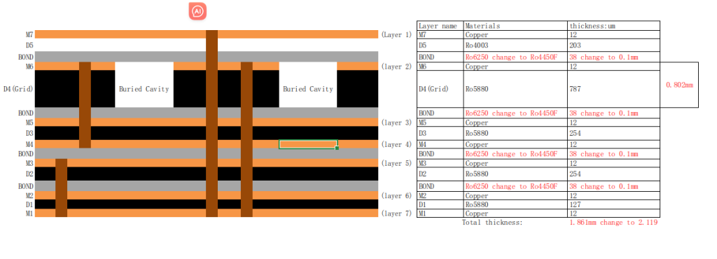
Antenna Cavity PCBs Manufacturer.As a leading Antenna Cavity PCBs manufacturer, we specialize in creating high-performance printed circuit boards designed for advanced antenna applications. Our expertise lies in precision engineering and cutting-edge manufacturing processes, ensuring optimal signal integrity and minimal interference. We provide custom solutions tailored to meet the demanding needs of industries like telecommunications, aerospace, and defense. With a commitment to quality and innovation, we deliver reliable, high-frequency Antenna Cavity PCBs that drive superior connectivity and performance in critical systems.
Antenna cavity PCBs (Printed Circuit Boards) are specialized circuit boards designed to integrate antennas within a cavity structure, optimizing the performance of RF (radio frequency) and microwave applications. These PCBs are essential in applications requiring high-frequency signal transmission, such as telecommunications, aerospace, and defense systems. This article explores the characteristics, design considerations, materials, manufacturing processes, applications, and advantages of antenna cavity PCBs.

What are Antenna Cavity PCBs?
Antenna cavity PCBs incorporate cavities within the PCB structure to house antennas, providing a controlled environment that enhances signal performance. These cavities are designed to optimize the electromagnetic properties, reduce signal loss, and improve the overall efficiency of the antenna. The integration of antennas within the PCB structure allows for compact and efficient designs, making them suitable for high-frequency applications.
Design Considerations for Antenna Cavity PCBs
Designing antenna cavity PCBs involves several critical considerations:
The shape, size, and placement of the cavity are crucial for optimizing the electromagnetic properties and performance of the antenna.
Choosing the right PCB materials that offer low dielectric loss, high thermal conductivity, and stable performance across frequencies is essential.
Ensuring proper impedance matching between the antenna and the rest of the circuitry is vital for minimizing signal reflection and loss.
Effective thermal management techniques must be implemented to dissipate heat generated by the high-frequency signals.
Proper shielding techniques are necessary to prevent electromagnetic interference (EMI) and ensure clean signal transmission.
Maintaining tight manufacturing tolerances is critical for ensuring consistent performance and reliability.
Materials Used in Antenna Cavity PCBs
Several materials are commonly used in the manufacturing of antenna cavity PCBs:
Materials such as Rogers RT/duroid, RO4000, and RO3000 series offer low dielectric loss and stable performance across high frequencies.
These materials provide excellent thermal and electrical properties, making them suitable for high-frequency applications.
Copper is used for conductive traces and cavity walls due to its excellent electrical conductivity.
TIMs, such as thermal grease or pads, are used to enhance heat transfer between components and cooling solutions.
Conductive materials, such as copper or aluminum, are used for shielding to prevent EMI.
Manufacturing Process of Antenna Cavity PCBs
The manufacturing process of antenna cavity PCBs involves several precise steps:
High-frequency laminates and other materials are prepared and processed into sheets or films.
Cavities are created within the PCB layers using precise machining or etching techniques.
The layers of the PCB, including the cavity, are stacked up according to the design, with careful consideration of the placement of dielectric materials and conductive traces.
Vias are drilled and plated to create vertical electrical connections between different layers and the cavity.
Components, including the antenna, are mounted on the PCB using automated surface mount technology (SMT) processes.
Heat sinks, cooling fans, and thermal interface materials are integrated to ensure effective thermal management.
Shielding materials are applied to prevent EMI and ensure clean signal transmission.
The assembled boards undergo rigorous testing and inspection to ensure they meet the required specifications for electrical performance, signal integrity, and reliability.
The tested and validated boards are assembled into their final form, packaged, and prepared for distribution.
Applications of Antenna Cavity PCBs
Antenna cavity PCBs are used in a wide range of high-frequency applications:
These PCBs are used in base stations, antennas, and other communication devices where high-frequency signal transmission is crucial.
Antenna cavity PCBs are essential in radar systems, satellite communication, and military electronics, where reliability and performance are critical.
These PCBs are used in medical imaging and diagnostic equipment that operate at high frequencies, requiring precise and reliable signal transmission.
Antenna cavity PCBs are used in advanced driver-assistance systems (ADAS), vehicle-to-everything (V2X) communication, and radar systems.
These PCBs are used in industrial sensors, automation systems, and other high-frequency industrial applications.
Advantages of Antenna Cavity PCBs
Antenna cavity PCBs offer several advantages:
The cavity structure minimizes signal loss and interference, improving signal strength and clarity.
Integrating antennas within the PCB allows for more compact designs, saving space and reducing the overall size of the device.
The controlled environment of the cavity protects the antenna from environmental factors, enhancing reliability and longevity.
These PCBs are designed to operate efficiently at high frequencies, making them suitable for RF and microwave applications.
Antenna cavity PCBs can be tailored to specific requirements, including frequency range, power handling, and environmental conditions.
FAQ
What are the key benefits of using antenna cavity PCBs?
The key benefits include enhanced signal performance, compact design, improved reliability, high-frequency capability, and customizability. These advantages make antenna cavity PCBs ideal for high-frequency and high-power applications.
What materials are commonly used in antenna cavity PCBs?
Common materials include high-frequency laminates such as Rogers RT/duroid, RO4000, and RO3000 series, ceramic-filled PTFE, copper for conductive traces and cavity walls, thermal interface materials (TIMs), and shielding materials such as copper or aluminum.
How does the design of an antenna cavity PCB ensure high performance?
The design ensures high performance by optimizing cavity design, selecting appropriate materials, ensuring proper impedance matching, implementing effective thermal management, applying proper shielding techniques, and maintaining tight manufacturing tolerances.
What are the common applications of antenna cavity PCBs?
Common applications include telecommunications (base stations, antennas), aerospace and defense (radar systems, satellite communication), medical devices (medical imaging, diagnostics), automotive electronics (ADAS, V2X communication), and industrial applications (sensors, automation systems). These PCBs are used in systems requiring high-frequency performance and reliable signal transmission.
 ALCANTA TECHNOLOGY(SHENZHEN)CO.,LTD