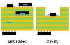
embedded-componet-pcb
Alcanta PCB offer Embedded Componet PCB, Cavities PCB, Embedded Componet PC boards, Embedded prats PC boards, From 4 layer to 50 layers. Advanced production technology.
Use Embedded Components To Improve PCB Performance And Reduce Size.Embedding discrete components within a PCB substrate is still considered cutting-edge, but advances in fabrication and EDA software have this technology on the rise.
The complexity and density of electronics design has increased, partly due to the rise of the mobile industry, introducing new challenges for printed-circuit board (PCB) designers. Embedding components within the board substrate offers a practical solution to several issues, and it’s quickly becoming a feasible production step for fabricators.
Why Embed Components?
Before discussing the methods for adding embedded components to a design, it is important to understand some of the advantages they offer. One must consider all the benefits and drawbacks of adding fabrication steps before starting the design, in addition to the potential effects on cost and production yield.
Reductions in size and cost drive innovation in PCB technology. Embedding components can help reduce the size of the board assembly. It also can potentially reduce the manufacturing cost for complex products.
Minimizing electrical path lengths to reduce parasitic effects is critical when dealing with high-frequency circuits. Reducing the wiring length of passive components to an IC can decrease parasitic capacitance and inductance, reducing load fluctuations and noise within the system. By embedding passive components, it’s possible to position them directly underneath the pin of an IC, minimizing potential negative effects, including via inductance.

Minimizing wiring length to an IC is a common solution for reducing parasitic effects and improving device performance. Embedding components in the board substrate (top) allows for additional wire length reduction over surface-mounting (bottom).
An integrated electromagnetic interference (EMI) shield can be manufactured directly around an embedded IC. Simply adding plated through-holes surrounding the IC can reduce capacitively and inductively coupled noise. It also can eliminate the need for an additional surface-mounted shield in certain applications.
Heat-conducting structures can be added to an embedded component easily, improving thermal management. One such example would be to embed thermal microvias in direct contact with an embedded component, allowing heat to dissipate to a thermal plane layer. Additionally, reducing the amount of PCB substrate that heat must travel through reduces thermal resistance.
Long-term reliability is a major source of difficulty and concern when implementing embedded components in a design. The sustainability of solder joints, when placed within the laminate framework of a PCB, is affected by subsequent soldering processes, such as reflow on surface-mount devices. Embedded components can cause additional problems after manufacturing, since they cannot be easily tested or replaced following a failure.
Types Of Embedded Components
Embedded components fall into two main categories, passive and active, but are largely used in different ways and for different purposes. Passives fill the large majority of components. Consequently, embedded capacitance and resistance has been studied comprehensively.
The term “embedded passive” does not generally refer to a discrete resistor or capacitor simply placed in a cavity within the board substrate. Rather, embedded passives are fabricated by choosing particular layer materials to form resistive or capacitive structures. While these types of embedded components were largely used at one point to save space, the development of smaller discrete passives have rendered them non-essential for that purpose in many designs.
Embedded passives still offer several benefits, including reduction of parasitic effects and size, and have become a common fabrication alternative to discrete surface-mount passives. This can be especially beneficial for applications such as series termination resistors, where hundreds of transmission lines enter dense ball-grid array (BGA) microprocessor and memory devices.
Manufacturing steps to place an IC within the board substrate can vary, but space must be created for the component body, in the form of a cavity. There are a few notable approaches to chip embedding technology:
Integrated module board (IMB): Components are aligned and placed inside a cavity that is routed to the core laminate by controlled-depth routing. The cavity is filled with molding polymer to ensure chemical, mechanical, and electrical compatibility with the substrate. Isotropic solder is impregnated with the polymer to form reliable solder joints when the embedded part is laminated into the stack.
Embedded wafer-level package (EWLP): All technology steps are performed at the wafer level. Fan-in is always required, meaning the area available for I/O is limited to the chip footprint size.
Embedded chip buildup (ECBU): Chips are mounted to polyimide film, and interconnect structures are built up from there.
Chip in polymer (CIP): Thin chips are embedded into buildup dielectric layers of PCBs, rather than integrating them into the core layers. Standard laminated substrate materials then can be used.
If you have any questions, please feel free to contact us with info@alcantapcb.com , we will be happy to help you.
 ALCANTA TECHNOLOGY(SHENZHEN)CO.,LTD