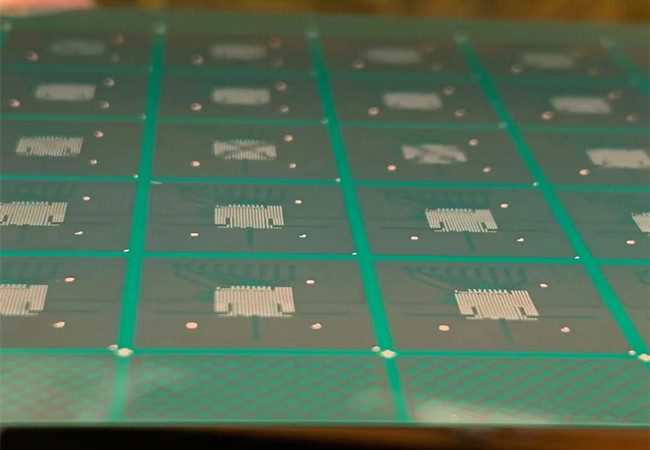
fc-bga-substrates
FC-BGA substrates (flip chip ball grid array) on a high density semiconductor package substrate allows high speed LSI chips with more functions. We have developed ultra high density wiring substrates with our original microfabrication and build-up wiring technologies, offering products supporting current semiconductor microfabrication.For a growing demand for LSIs for automotive SoC or high-end processors (server, AI, network) as well as for PCs or game devices, we provide comprehensive support from substrate design to production.Solutions for lead-free and halogen-free products are also available.
FC-BGA substrate are semiconductor packages with fine design rule and high reliability. Alcanta PCB company provides IC packages with more than 2,000 I/Os, and which comply with next generation flip-chip LSI utilizing cutting-edge design rule and state-of-the-art processing technology.

Features
Leaders-in circuitization rule as line/space: 9µm/12µm
Advanced small via formation with laser via technology
Highly reliable thermosetting epoxy used
Various surface finish options available (Ni/Au, SAC soldering, etc.)
Applicable environmentally-friendly products (Halogen-free, Lead-free)
Specifications
Item Specification Note
Layer Structure Up to 9-n-9
Build-up Line Width / Space 9μm / 12μm
Via Land Diameter 85μm
Core Line Width (Subtractive) 30μm
Core Space (Subtractive) 40μm
Flip Chip Pitch 125μm
Applications
ASICs for servers / routers
MPUs for high performance game consoles
Graphics processors, etc.
If you have any questions, please feel free to contact us with info@alcantapcb.com , we will be happy to help you.
 ALCANTA TECHNOLOGY(SHENZHEN)CO.,LTD